
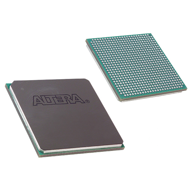
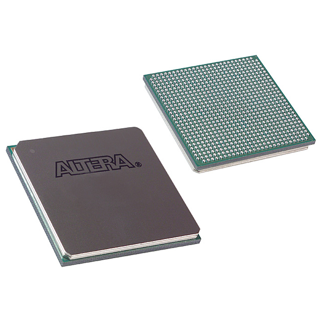
10AX032E1F27E1HG
| Part Description |
Arria 10 GX Field Programmable Gate Array (FPGA) IC 240 21040128 320000 672-BBGA, FCBGA |
|---|---|
| Quantity | 435 Available (as of June 8, 2026) |

| Product Category | Field Programmable Gate Array (FPGA) |
|---|---|
| Manufacturer | Intel |
| Manufacturing Status | Active |
| Manufacturer Standard Lead Time | 16 Weeks |
| Datasheet |
Specifications & Environmental
| Device Package | 672-FBGA (27x27) | Grade | Extended | Operating Temperature | 0°C – 100°C | ||
|---|---|---|---|---|---|---|---|
| Package / Case | 672-BBGA, FCBGA | Number of I/O | 240 | Voltage | 870 mV - 980 mV | ||
| Mounting Method | Surface Mount | RoHS Compliance | RoHS Compliant | REACH Compliance | REACH Unaffected | ||
| Moisture Sensitivity Level | 3 (168 Hours) | Number of LABs/CLBs | 119900 | Number of Logic Elements/Cells | 320000 | ||
| Number of Gates | N/A | ECCN | 5A002A1 | HTS Code | 8542.39.0001 | ||
| Qualification | N/A | Total RAM Bits | 21040128 |
Overview of 10AX032E1F27E1HG – Arria 10 GX FPGA (672-FBGA, 320,000 logic elements)
The 10AX032E1F27E1HG is an Intel Arria 10 GX field-programmable gate array (FPGA) in a 672-BBGA (672-FBGA, 27×27) surface-mount package. It combines high logic density and on-chip memory with mid-range, power-conscious architecture suited to demanding communications, data center, broadcast and imaging applications.
As part of the Intel Arria 10 device family, this device leverages the series' focus on higher performance and power efficiency for mid-range FPGA and SoC use cases, and includes architectural elements such as adaptive logic modules, variable-precision DSP resources, embedded memory blocks and advanced clocking and transceiver capabilities described in the Arria 10 overview.
Key Features
- Logic Density Provides 320,000 logic elements to implement complex digital functions and custom accelerators.
- On-chip Memory Includes 21,040,128 total RAM bits for embedded buffering, state storage and high-bandwidth local data paths.
- I/O Capacity 240 user I/O pins support broad external connectivity for interfaces and memory bus implementations.
- Advanced FPGA Architecture Part of the Intel Arria 10 family featuring adaptive logic modules and variable-precision DSP blocks for flexible compute and signal-processing tasks.
- Serial and Protocol Support (Series Capabilities) Arria 10 devices include low-power serial transceivers, enhanced PCS hard IP for Interlaken and 10 Gbps Ethernet, and PCIe Gen1/Gen2/Gen3 hard IP as described in the device overview.
- Clocking and PLLs Comprehensive clock networks and fractional-synthesis I/O/PLL resources are part of the Arria 10 architecture to support complex timing domains and high-speed interfaces.
- Power and Supply Specified operating core voltage range is 870 mV to 980 mV, enabling designs targeting the Arria 10 family power envelope.
- Package & Mounting 672-BBGA, FCBGA package (supplier device package: 672-FBGA, 27×27) in a surface-mount form factor for compact PCB integration.
- Operating Range & Grade Extended-grade device rated for 0 °C to 100 °C operation; RoHS compliant.
- Reliability & System Features (Series Capabilities) Arria 10 device documentation describes support for SEU error detection and correction, dynamic and partial reconfiguration, and power management features to support robust system designs.
Typical Applications
- Wireless Infrastructure Channel and switch cards in remote radio heads and mobile backhaul systems that need programmable logic and on-chip memory.
- High‑Speed Networking Line cards, muxponders and transponders for 40G/100G and aggregation systems using the device family's transceiver and protocol hard IP capabilities.
- Broadcast & Professional AV Studio switches, video transport and conferencing equipment benefiting from high logic density and on-chip buffering.
- Compute & Storage Acceleration Flash cache, cloud server acceleration and custom data-path implementations that leverage embedded RAM and DSP resources.
- Medical & Imaging Diagnostic imaging and scanning equipment that require programmable signal processing and deterministic I/O handling.
Unique Advantages
- High Logic Capacity: 320,000 logic elements enable large, integrated designs and complex control or acceleration functions within a single device.
- Substantial On‑Chip Memory: Over 21 million bits of embedded RAM reduce external memory dependency and improve data-path latency.
- Wide I/O Reach: 240 I/O pins provide flexibility for multiple interfaces and external memories without immediate need for additional multiplexing logic.
- Compact, Board‑Ready Package: 672-FBGA (27×27) surface-mount package supports dense PCB layouts for space-constrained systems.
- Arria 10 Series Capabilities: Architectural features such as DSP blocks, clocking resources, transceivers and protocol hard IP (PCIe, Ethernet, Interlaken) simplify implementation of communications and compute subsystems.
- Extended‑Grade Operation: Rated for 0 °C to 100 °C to meet a range of commercial and enterprise deployment environments.
Why Choose 10AX032E1F27E1HG?
The 10AX032E1F27E1HG brings Arria 10 family architecture into a high-density, mid-range FPGA package that balances logic capacity, embedded memory and I/O for communications, data center acceleration and advanced imaging systems. Its combination of 320,000 logic elements, 21,040,128 RAM bits and 240 I/Os in a 672-FBGA footprint makes it a compelling option for designers who need a programmable, integrated building block without proliferating discrete components.
Supported by Arria 10 series-level features—such as adaptive logic modules, DSP resources, transceivers and hard IP for common protocols—this device provides a scalable platform for teams developing mid-range, power-conscious solutions with established device-family documentation and development flows.
Request a quote or submit an availability inquiry to receive pricing and lead-time information for the 10AX032E1F27E1HG.


Date Founded: 1968
Headquarters: Santa Clara, California, USA
Employees: 130,000+
Revenue: $54.23 Billion
Certifications and Memberships: ISO9001:2015, ISO14001:2015, ISO17025:2017, ISO27001:2022, ISO45001:2018, ISO50001:2018


