
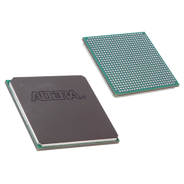
10AX027H4F35E3SG
| Part Description |
Arria 10 GX Field Programmable Gate Array (FPGA) IC 384 17870848 270000 1152-BBGA, FCBGA |
|---|---|
| Quantity | 1,000 Available (as of June 18, 2026) |

| Product Category | Field Programmable Gate Array (FPGA) |
|---|---|
| Manufacturer | Intel |
| Manufacturing Status | Active |
| Manufacturer Standard Lead Time | 16 Weeks |
| Datasheet |
Specifications & Environmental
| Device Package | 1152-FBGA, FC (35x35) | Grade | Extended | Operating Temperature | 0°C – 100°C | ||
|---|---|---|---|---|---|---|---|
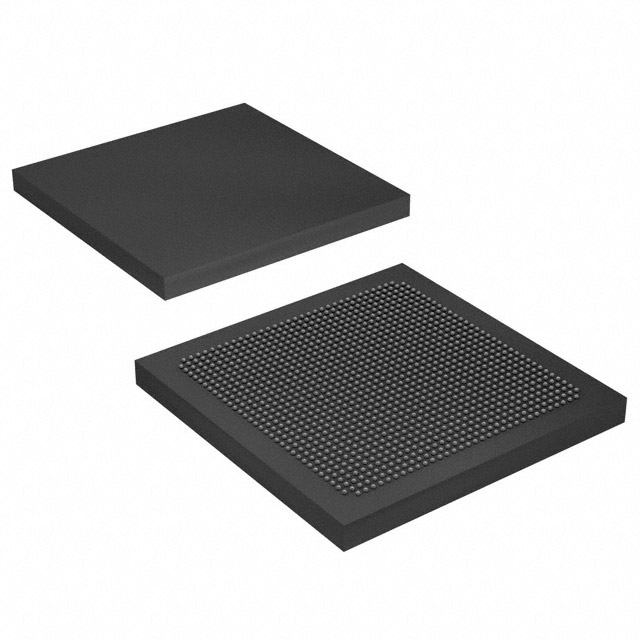
| Package / Case | 1152-BBGA, FCBGA | Number of I/O | 384 | Voltage | 870 mV - 980 mV | ||
| Mounting Method | Surface Mount | RoHS Compliance | RoHS Compliant | REACH Compliance | REACH Unaffected | ||
| Moisture Sensitivity Level | 3 (168 Hours) | Number of LABs/CLBs | 101620 | Number of Logic Elements/Cells | 270000 | ||
| Number of Gates | N/A | ECCN | 5A002A1 | HTS Code | 8542.39.0001 | ||
| Qualification | N/A | Total RAM Bits | 17870848 |
Overview of 10AX027H4F35E3SG – Arria 10 GX FPGA, 270,000 Logic Elements, 1152-BBGA
The 10AX027H4F35E3SG is an Intel Arria 10 GX field-programmable gate array (FPGA) IC offering 270,000 logic elements in a 1152-BBGA (FCBGA) package. It integrates 17,870,848 bits of on-chip RAM and 384 user I/O pins to support mid-range, high-performance, power-efficient designs.
Part of the Arria 10 device family (20 nm), this device targets markets including wireless and wireline infrastructure, broadcast, computing and storage, medical imaging, and defense, where a balance of performance, integration, and power efficiency is required.
Key Features
- Logic Capacity 270,000 logic elements providing programmable logic resources for complex custom hardware acceleration and system control.
- On-Chip Memory 17,870,848 total RAM bits for large buffering, packet processing, or on-chip data storage.
- IO and Connectivity 384 user I/O pins to connect diverse high-speed and parallel interfaces; family-level support includes PCIe Gen1/2/3 and 10 Gbps Ethernet hard IP options.
- Transceivers and SerDes Arria 10 family features include low-power serial transceivers and enhanced PCS hard IP suitable for high-speed serial links.
- DSP and Clocking Variable-precision DSP block and extensive clock network and PLL sources (family-level), enabling flexible signal processing and timing architectures.
- Package & Mounting 1152-BBGA FCBGA package (supplier package: 1152-FBGA, FC 35×35) with surface-mount assembly for compact board integration.
- Power Core supply range 870 mV to 980 mV to match platform power design requirements.
- Temperature & Grade Extended grade device with an operating temperature range of 0 °C to 100 °C.
- Compliance RoHS compliant.
Typical Applications
- Wireless Infrastructure Channel processing and backhaul equipment that need programmable logic and on-chip memory for adaptable signal processing and timing.
- Wireline Networking Line cards, muxponders and transponders that leverage integrated transceivers and high-density I/O for multi-gigabit packet forwarding and aggregation.
- Broadcast and Video Studio switching and video transport where large on-chip RAM and flexible DSP resources support video buffering, format conversion, and routing.
- Computing & Storage Acceleration Server acceleration and flash-cache controllers that require programmable logic, memory, and high-speed interfaces for custom data-paths.
- Medical & Defense Systems Diagnostic imaging, radar, and secure communications applications that benefit from configurable DSP blocks and dense logic resources.
Unique Advantages
- Balanced Performance and Efficiency: The Arria 10 family is described as delivering higher performance with power-efficiency, making the device suitable for power-sensitive mid-range applications.
- High Integration Density: 270,000 logic elements and nearly 18 Mb of on-chip RAM reduce external component count and simplify board design.
- Flexible Connectivity: 384 I/O pins combined with family-level hard IP for PCIe and multi-gigabit Ethernet simplify integration of high-speed interfaces.
- Scalable DSP and Memory Resources: Variable-precision DSP blocks and multiple embedded memory configurations enable optimized implementations for signal processing and buffering.
- Robust Packaging Options: 1152-BBGA FCBGA (35×35) surface-mount package supports dense board layouts while maintaining thermal and mechanical stability for production assemblies.
- Industry Compliance: RoHS compliance supports environmental and regulatory requirements for commercial deployments.
Why Choose 10AX027H4F35E3SG?
The 10AX027H4F35E3SG positions itself as a capable mid-range FPGA that combines substantial programmable logic, large on-chip memory, and extensive I/O in a compact FCBGA package. Its placement within the Arria 10 family emphasizes a balance of performance and power efficiency for applications that require adaptable hardware acceleration without sacrificing energy profile.
This device suits engineers and system designers building wireless and wireline infrastructure, broadcast/video processing, compute/storage acceleration, and imaging or defense systems who require a scalable, supported FPGA platform with family-level IP for high-speed interfaces and DSP-heavy workloads.
Request a quote or submit an inquiry to purchase the 10AX027H4F35E3SG and discuss availability and pricing for your design requirements.


Date Founded: 1968
Headquarters: Santa Clara, California, USA
Employees: 130,000+
Revenue: $54.23 Billion
Certifications and Memberships: ISO9001:2015, ISO14001:2015, ISO17025:2017, ISO27001:2022, ISO45001:2018, ISO50001:2018


