
10AX032E2F27E2SG
| Part Description |
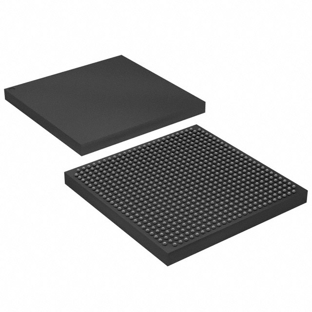
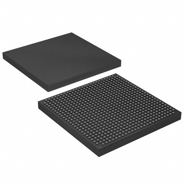
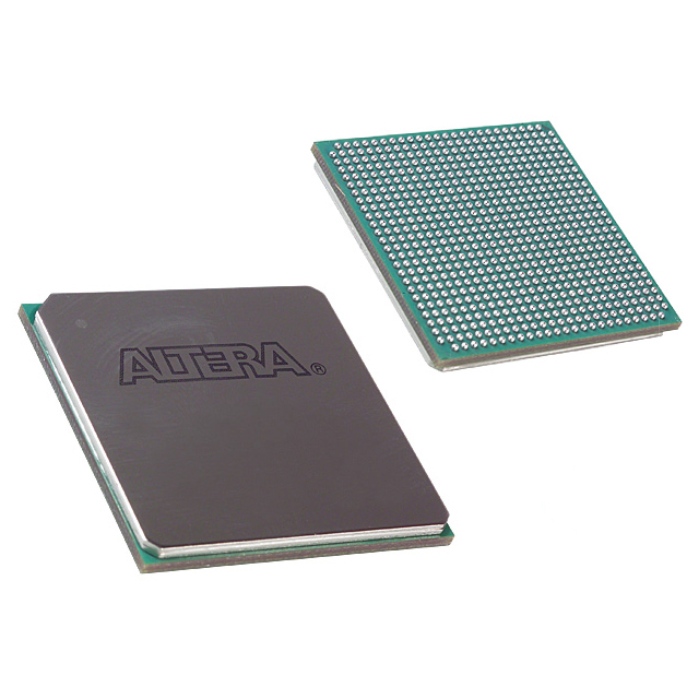
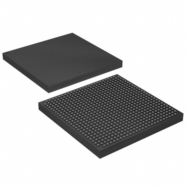
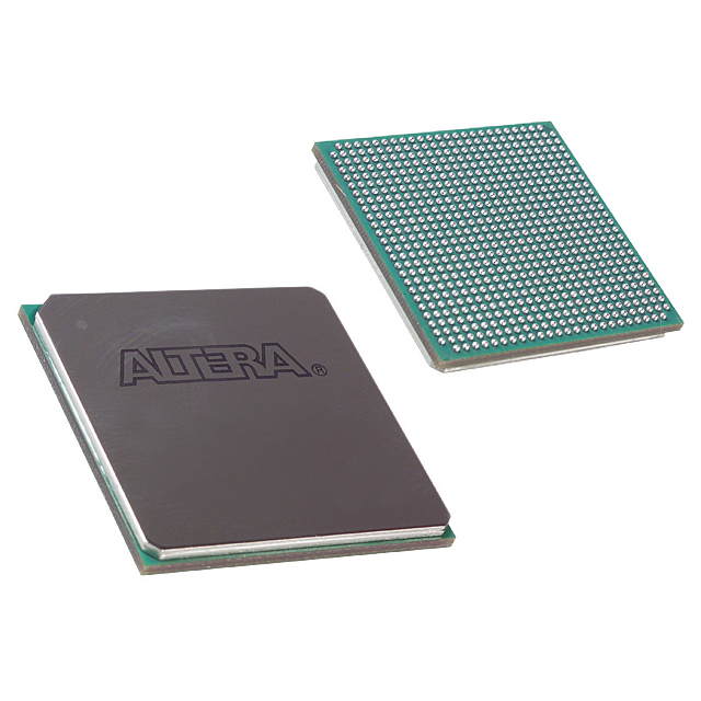
Arria 10 GX Field Programmable Gate Array (FPGA) IC 240 21040128 320000 672-BBGA, FCBGA |
|---|---|
| Quantity | 1,593 Available (as of October 8, 2026) |
| Product Category | Field Programmable Gate Array (FPGA) |
|---|---|
| Manufacturer | Intel |
| Manufacturing Status | Active |
| Manufacturer Standard Lead Time | 16 Weeks |
| Datasheet |
Specifications & Environmental
| Device Package | 672-FBGA, FC (27x27) | Grade | Extended | Operating Temperature | 0°C – 100°C | ||
|---|---|---|---|---|---|---|---|
| Package / Case | 672-BBGA, FCBGA | Number of I/O | 240 | Voltage | 870 mV - 980 mV | ||
| Mounting Method | Surface Mount | RoHS Compliance | RoHS Compliant | REACH Compliance | REACH Unaffected | ||
| Moisture Sensitivity Level | 3 (168 Hours) | Number of LABs/CLBs | 119900 | Number of Logic Elements/Cells | 320000 | ||
| Number of Gates | N/A | ECCN | 5A002A1 | HTS Code | 8542.39.0001 | ||
| Qualification | N/A | Total RAM Bits | 21040128 |
Overview of 10AX032E2F27E2SG – Arria 10 GX Field Programmable Gate Array (FPGA) IC 240 I/Os, 320,000 Logic Elements, 21,040,128 Bits RAM, 672-BBGA
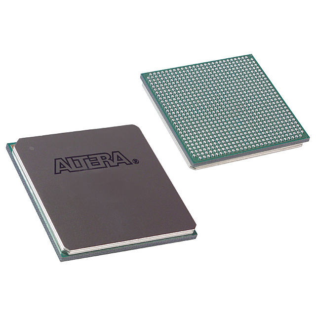
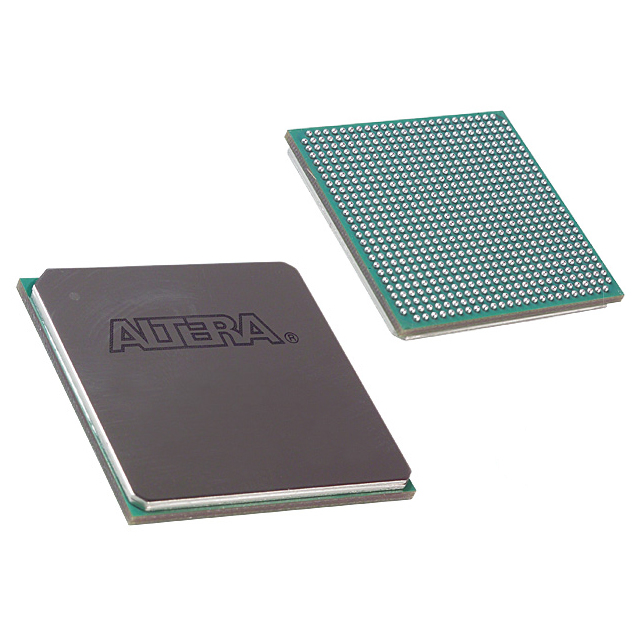
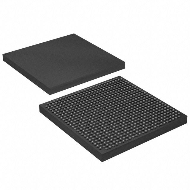
The 10AX032E2F27E2SG is an Intel Arria 10 GX field programmable gate array (FPGA) in a 672-ball FCBGA package. It is a 20 nm mid-range FPGA optimized for high-performance, power-sensitive designs across communications, broadcast, computing, medical and defense markets.
This device combines high logic density, substantial embedded RAM, and a wide I/O count to enable complex midrange system functions while operating within a low-voltage supply range and an extended temperature window.
Key Features
- Logic Capacity — 320,000 logic elements to implement large-scale programmable logic and custom processing functions.
- Embedded Memory — 21,040,128 total RAM bits for on-chip buffering, packet processing, and state storage.
- I/O Density — 240 device I/Os to support wide parallel interfaces and multiple external peripherals or memory channels.
- Process and Architecture — Part of the Intel Arria 10 family based on 20 nm technology, targeting midrange applications that require a balance of performance and power efficiency.
- Power Supply — Operates from 870 mV to 980 mV supply rails, supporting low-voltage system integration.
- Package & Mounting — 672-ball BBGA (FCBGA), supplier package 672-FBGA (27×27), surface-mount for compact board-level implementation.
- Operating Range & Grade — Extended grade with operating temperature from 0 °C to 100 °C for a broad set of commercial and industrial-adjacent environments.
- Compliance — RoHS compliant to meet standard environmental requirements.
Typical Applications
- Wireless Infrastructure: Channel and switch cards or mobile backhaul equipment where high logic density and on-chip memory support signal processing and control functions.
- Wireline Networking: 40G/100G muxponders, transponders, and line cards that benefit from extensive I/O and on-chip buffering.
- Broadcast and Media: Studio switches, video conferencing, and professional audio/video processing using the device’s logic and memory resources for real-time data handling.
- Computing & Storage Acceleration: Server acceleration and flash cache applications that leverage programmable logic and embedded RAM for custom acceleration tasks.
Unique Advantages
- High Logic Density: 320,000 logic elements provide the capacity to consolidate multiple functions into a single device, reducing board-level complexity.
- Significant On-Chip Memory: Over 21 million RAM bits enable sizable buffering and local data storage, improving throughput for streaming and packet-based designs.
- Robust I/O Count: 240 I/Os allow flexible interfacing to external devices, memory, and high-speed lanes without excessive external components.
- Compact, Surface-Mount Package: 672-ball FCBGA supports dense board layouts and high pin-count integration in a 27×27 supplier package footprint.
- Extended Grade and RoHS Compliance: Rated for 0 °C to 100 °C operation and RoHS compliant for broad deployment and regulatory alignment.
- Family-Level Resources: As part of the Intel Arria 10 family, the device benefits from published device documentation and development resources.
Why Choose 10AX032E2F27E2SG?
The 10AX032E2F27E2SG positions as a high-capacity, midrange FPGA suited to designs that require substantial programmable logic, considerable embedded RAM, and broad I/O connectivity within a compact FCBGA package. Its low-voltage operation and extended temperature rating make it appropriate for power-sensitive systems and a range of deployment environments.
Engineers designing communications, media processing, compute acceleration, or storage interfaces will find this device delivers the integration and flexibility needed to reduce system BOM and accelerate time-to-market, backed by the Intel Arria 10 device family documentation and resources.
Request a quote or submit an inquiry for pricing and availability to begin integrating the 10AX032E2F27E2SG into your design.





















Date Founded: 1968
Headquarters: Santa Clara, California, USA
Employees: 130,000+
Revenue: $54.23 Billion
Certifications and Memberships: ISO9001:2015, ISO14001:2015, ISO17025:2017, ISO27001:2022, ISO45001:2018, ISO50001:2018


