
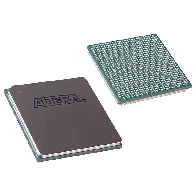
10AX032E2F27I1SG
| Part Description |
Arria 10 GX Field Programmable Gate Array (FPGA) IC 240 21040128 320000 672-BBGA, FCBGA |
|---|---|
| Quantity | 620 Available (as of June 15, 2026) |

| Product Category | Field Programmable Gate Array (FPGA) |
|---|---|
| Manufacturer | Intel |
| Manufacturing Status | Discontinued |
| Manufacturer Standard Lead Time | 13 Weeks |
| Datasheet |
Specifications & Environmental
| Device Package | 672-FBGA (27x27) | Grade | Industrial | Operating Temperature | -40°C – 100°C | ||
|---|---|---|---|---|---|---|---|
| Package / Case | 672-BBGA, FCBGA | Number of I/O | 240 | Voltage | 870 mV - 980 mV | ||
| Mounting Method | Surface Mount | RoHS Compliance | RoHS Compliant | REACH Compliance | REACH Unaffected | ||
| Moisture Sensitivity Level | 3 (168 Hours) | Number of LABs/CLBs | 119900 | Number of Logic Elements/Cells | 320000 | ||
| Number of Gates | N/A | ECCN | 5A002A1 | HTS Code | 8542.39.0001 | ||
| Qualification | N/A | Total RAM Bits | 21040128 |
Overview of 10AX032E2F27I1SG – Arria 10 GX Field Programmable Gate Array (FPGA) IC
The 10AX032E2F27I1SG is an Intel Arria 10 GX field programmable gate array (FPGA) offered in a 672-ball FCBGA package. It is part of the 20 nm Arria 10 device family designed for mid-range, performance-sensitive applications that require a balance of compute density and power efficiency.
Typical markets and use cases include wireless and wireline infrastructure, broadcast and video systems, compute and storage acceleration, medical imaging, and defense communications where programmable logic, embedded memory, and high-speed I/O integration are required.
Key Features
- Core Logic 320,000 logic elements provide substantial programmable logic capacity for complex custom hardware implementations.
- Embedded Memory 21,040,128 total RAM bits of on-chip memory to support buffering, lookup tables, and on-chip data storage.
- I/O Count 240 I/O pins to interface with external peripherals, memory, and high-speed transceivers.
- Transceivers and Interfaces Arria 10 GX family-level features include high-speed serial transceivers, hard IP for PCIe Gen1/2/3, and protocol support such as 10 Gbps Ethernet and Interlaken (as described in the device family overview).
- DSP and Compute Blocks Variable-precision DSP blocks (documented for the Arria 10 family) enable efficient implementation of signal-processing and numeric workloads.
- Clocking and PLLs Rich clock network and PLL resources for flexible clock synthesis and domain management, as described in the family overview.
- Power Supply Core voltage supply range of 870 mV to 980 mV to support the device’s power requirements.
- Package and Mounting 672-ball FCBGA package (27 × 27 mm supplier package) designed for surface-mount assembly.
- Temperature Grade Industrial-grade operation from −40 °C to 100 °C for deployment in demanding environments.
- Standards and Ecosystem Part of the Intel Arria 10 family, which includes device-level features such as dynamic and partial reconfiguration and integrated system-level capabilities (refer to family documentation).
Typical Applications
- Wireless Infrastructure Channel processing, remote radio head functions, and mobile backhaul where programmable logic and DSP capacity accelerate baseband and control functions.
- Wireline and Telecom Line cards, muxponders, and transponders (including 40G/100G applications) that require high-speed serial interfaces and on-chip protocol IP.
- Broadcast and Video Studio switching, video transport, and conferencing systems that benefit from embedded memory and real-time processing resources.
- Compute and Storage Acceleration Flash cache, server acceleration, and cloud compute offload tasks leveraging FPGA compute density and memory bandwidth.
- Medical and Defense Systems Diagnostic imaging, radar, and secure communications where industrial temperature range and programmable logic flexibility are important.
Unique Advantages
- Substantial Logic Capacity: 320,000 logic elements enable implementation of complex custom hardware functions without external ASICs.
- On-Chip Memory for High-Bandwidth Tasks: Over 21 million RAM bits provide local storage for buffering and algorithm acceleration, reducing off-chip memory dependence.
- High-Speed I/O and Protocol Support: 240 I/Os combined with Arria 10 family transceiver and protocol IP options simplify integration into high-throughput systems.
- Industrial Temperature Range: −40 °C to 100 °C operation supports deployment in industrial and other temperature-demanding environments.
- Power-Managed Operation: Documented family-level power-efficiency features and a defined core voltage range (870–980 mV) help designers optimize power vs. performance.
- Package for Production Assembly: 672-ball FCBGA (27 × 27 mm) package supports standard surface-mount PCB assembly for production systems.
Why Choose 10AX032E2F27I1SG?
The 10AX032E2F27I1SG delivers a balance of programmable logic density, embedded memory, and industrial-grade operating range suitable for mid-range systems that require configurable hardware acceleration and flexible I/O. As a member of the Intel Arria 10 GX family, it brings documented family-level capabilities—such as variable-precision DSP resources, advanced clocking, and high-speed protocol support—that help shorten design cycles and enable scalable system architectures.
This device is well suited to engineers and system designers building wireless/wireline infrastructure, broadcast/video processing, compute/storage accelerators, and ruggedized equipment where on-chip memory, logic capacity, and industrial temperature support are key selection criteria.
Request a quote or contact sales to discuss availability, pricing, and how the 10AX032E2F27I1SG can fit your next FPGA-based design.


Date Founded: 1968
Headquarters: Santa Clara, California, USA
Employees: 130,000+
Revenue: $54.23 Billion
Certifications and Memberships: ISO9001:2015, ISO14001:2015, ISO17025:2017, ISO27001:2022, ISO45001:2018, ISO50001:2018


