
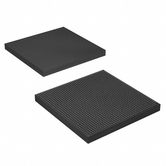
10AX066K3F40E2SG
| Part Description |
Arria 10 GX Field Programmable Gate Array (FPGA) IC 696 49610752 660000 1517-BBGA, FCBGA |
|---|---|
| Quantity | 192 Available (as of June 15, 2026) |
| Product Category | Field Programmable Gate Array (FPGA) |
|---|---|
| Manufacturer | Intel |
| Manufacturing Status | Active |
| Manufacturer Standard Lead Time | 12 Weeks |
| Datasheet |
Specifications & Environmental
| Device Package | 1517-FCBGA (40x40) | Grade | Extended | Operating Temperature | 0°C – 100°C | ||
|---|---|---|---|---|---|---|---|
| Package / Case | 1517-BBGA, FCBGA | Number of I/O | 696 | Voltage | 870 mV - 930 mV | ||
| Mounting Method | Surface Mount | RoHS Compliance | RoHS Compliant | REACH Compliance | REACH Unaffected | ||
| Moisture Sensitivity Level | 3 (168 Hours) | Number of LABs/CLBs | 250540 | Number of Logic Elements/Cells | 660000 | ||
| Number of Gates | N/A | ECCN | 3A001A7B | HTS Code | 8542.39.0001 | ||
| Qualification | N/A | Total RAM Bits | 49610752 |
Overview of 10AX066K3F40E2SG – Arria 10 GX FPGA, 1517-FCBGA (Extended Grade)
The 10AX066K3F40E2SG is an Intel Arria 10 GX field-programmable gate array (FPGA) provided in a 1517-ball FCBGA package for surface-mount applications. It combines a high logic capacity and large embedded memory with the Arria 10 device family architecture to address mid-range, performance-sensitive designs.
Target markets include wireless and wireline communications, broadcast, computing and storage, medical, and military applications. Key value propositions are high integration, performance-oriented FPGA fabric, and platform features such as flexible clocking, transceivers, and embedded memory as described in the Arria 10 device overview.
Key Features
- Logic Capacity Provides 660,000 logic elements to implement complex digital designs and large FPGA-based systems.
- Embedded Memory Includes 49,610,752 total RAM bits to support on-chip buffering, working memory, and local storage for high-throughput data processing.
- I/O Density Up to 696 user I/Os to support wide bus interfaces and dense external connectivity in a single package.
- Transceivers and High‑Speed Interfaces Arria 10 device family features low-power serial transceivers and support for high-speed protocols such as 10 Gbps Ethernet and PCIe Gen1/Gen2/Gen3 hard IP as documented in the device overview.
- Adaptive Logic and DSP Architecture includes adaptive logic modules and variable‑precision DSP blocks for optimized arithmetic and signal-processing implementations.
- Clocking and PLLs Comprehensive clock networks with fractional synthesis and I/O PLLs for flexible clock distribution and timing control across the design.
- Configuration and Reconfiguration Supports dynamic and partial reconfiguration options described for Arria 10 devices to enable in-field updates and runtime reconfiguration.
- Package and Mounting 1517‑BBGA / 1517‑FCBGA (40×40) surface-mount package for high-pin-count board integration.
- Power and Operating Range Specified supply voltage range of 870 mV to 930 mV and operating temperature range of 0 °C to 100 °C; RoHS compliant and labeled as Extended grade.
Typical Applications
- Wireless Infrastructure Channel and switch cards for remote radio heads and mobile backhaul deployments where FPGA logic and transceiver integration accelerate RF and baseband tasks.
- Wireline Communications 40G/100G muxponders, transponders, and line cards that require high-speed interfaces, large on-chip memory, and PCIe/ethernet hard IP.
- Broadcast and Media Studio switches, video transport, and professional audio/video processing that leverage the device’s DSP blocks and large memory for real-time media pipelines.
- Computing and Storage Flash cache controllers, server acceleration, and cloud compute offload that use the FPGA’s logic density and I/O count for custom acceleration and data-path processing.
- Medical and Defense Diagnostic imaging and radar/defense signal-processing where reconfigurable logic and on-chip memory support algorithm acceleration and system flexibility.
Unique Advantages
- High integration density: The combination of 660,000 logic elements and nearly 50 million RAM bits reduces the need for external components and simplifies complex system designs.
- Broad interface support: 696 I/Os plus documented support for PCIe and 10 Gbps Ethernet hard IP enable direct connection to high-speed networks and peripherals.
- Flexible clock and transceiver subsystems: Comprehensive clock networks, fractional synthesis PLLs, and low-power serial transceivers allow designers to meet diverse timing and protocol requirements.
- Reconfiguration capabilities: Dynamic and partial reconfiguration options provide in-field adaptability to update or optimize designs without full device replacement.
- Extended grade and package options: Extended-grade temperature range and a 1517-FCBGA surface-mount package support deployment in demanding board-level applications.
- Documented platform features: The Arria 10 device overview details DSP blocks, adaptive logic modules, memory types, and power-management features to support engineering evaluation and design planning.
Why Choose 10AX066K3F40E2SG?
The 10AX066K3F40E2SG Arria 10 GX FPGA balances large programmable logic capacity, substantial embedded memory, and extensive I/O in a high‑pin‑count FCBGA package. It is positioned for engineers developing mid-range, performance-sensitive systems that require on-chip acceleration, flexible connectivity, and the ability to reconfigure logic in the field.
Design teams and procurement professionals will find this device suitable for projects that demand scalability and integration—leveraging Arria 10 architecture features such as DSP blocks, clocking resources, transceivers, and supported high-speed protocol hard IP to shorten development and optimize system BOM.
If you would like pricing, availability, or to request a formal quote for 10AX066K3F40E2SG, submit a request for a quote or contact the supplier’s sales channel with your requirements and quantity.


Date Founded: 1968
Headquarters: Santa Clara, California, USA
Employees: 130,000+
Revenue: $54.23 Billion
Certifications and Memberships: ISO9001:2015, ISO14001:2015, ISO17025:2017, ISO27001:2022, ISO45001:2018, ISO50001:2018


