
10M04DCU324C8G
| Part Description |
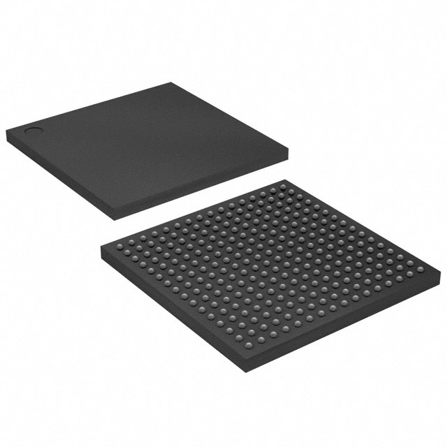
MAX® 10 Field Programmable Gate Array (FPGA) IC 246 193536 4000 324-LFBGA |
|---|---|
| Quantity | 432 Available (as of June 15, 2026) |

| Product Category | Field Programmable Gate Array (FPGA) |
|---|---|
| Manufacturer | Intel |
| Manufacturing Status | Active |
| Manufacturer Standard Lead Time | 16 Weeks |
| Datasheet |
Specifications & Environmental
| Device Package | 324-UBGA (15x15) | Grade | Commercial | Operating Temperature | 0°C – 85°C | ||
|---|---|---|---|---|---|---|---|
| Package / Case | 324-LFBGA | Number of I/O | 246 | Voltage | 1.15 V - 1.25 V | ||
| Mounting Method | Surface Mount | RoHS Compliance | RoHS Compliant | REACH Compliance | REACH Unaffected | ||
| Moisture Sensitivity Level | 3 (168 Hours) | Number of LABs/CLBs | 250 | Number of Logic Elements/Cells | 4000 | ||
| Number of Gates | N/A | ECCN | 3A991D | HTS Code | 8542.39.0001 | ||
| Qualification | N/A | Total RAM Bits | 193536 |
Overview of 10M04DCU324C8G – MAX® 10 Field Programmable Gate Array (FPGA) IC 246 193536 4000 324-LFBGA
The 10M04DCU324C8G is a MAX® 10 field programmable gate array (FPGA) from Intel, presented in a compact 324-LFBGA package. It provides a balance of programmable logic, on-chip RAM, and flexible I/O for commercial-grade embedded designs.
With 4,000 logic elements, 193,536 bits of on-chip RAM, and up to 246 I/O pins, this device is suited for applications that require moderate logic density and significant I/O connectivity while operating within a 0 °C to 85 °C commercial temperature range.
Key Features
- Core Architecture: MAX® 10 FPGA from Intel, delivering reprogrammable logic in a single-chip solution.
- Logic Capacity: 4,000 logic elements implemented across 250 LABs, enabling a range of mid-density logic designs.
- On-Chip Memory: 193,536 total RAM bits for embedded data buffering, state machines, and small LUT-based memories.
- I/O Resources: Up to 246 I/O pins to support multiple parallel interfaces and system-level connectivity.
- Power: Core voltage supply range of 1.15 V to 1.25 V for the device core supply requirements.
- Package & Mounting: 324-LFBGA package (supplier device package 324-UBGA, 15×15) with surface-mount mounting for compact board placement.
- Grade & Temperature: Commercial grade with an operating temperature range from 0 °C to 85 °C.
- Environmental Compliance: RoHS compliant, supporting lead-free manufacturing processes.
Typical Applications
- Embedded Control: Use the device’s 4,000 logic elements and on-chip RAM to implement control algorithms, state machines, and timing-critical logic for commercial embedded systems.
- Interface Bridging: Leverage up to 246 I/Os to implement protocol translation, glue logic, and parallel/serial interface aggregation between subsystems.
- User Interface and Display Control: Deploy the device to manage display drivers, touch controllers, and HMI logic where moderate logic density and flexible I/O are required.
- Prototyping and Development: Ideal for developers needing a reprogrammable platform with substantial RAM and I/O capacity in a compact package for proof-of-concept and evaluation.
Unique Advantages
- Balanced Logic and Memory: 4,000 logic elements paired with 193,536 bits of on-chip RAM supports combined control and buffering functions without external memory in many designs.
- High I/O Count: 246 I/Os enable broad connectivity to sensors, peripherals, and external controllers, reducing the need for additional interface chips.
- Compact, Surface-Mount Package: 324-LFBGA (324-UBGA, 15×15) offers a space-efficient footprint for dense board designs while maintaining necessary signals.
- Low-Voltage Core Support: 1.15 V–1.25 V supply range supports modern low-voltage system architectures.
- Commercial Temperature Range: Rated 0 °C to 85 °C for applications targeted at commercial-environment products.
- RoHS Compliant: Meets environmental requirements for lead-free production and assembly.
Why Choose 10M04DCU324C8G?
The 10M04DCU324C8G positions itself as a compact, commercially rated FPGA solution that combines moderate logic capacity, substantial on-chip RAM, and a high I/O count in a 324-LFBGA surface-mount package. Its specification set makes it appropriate for embedded control, interface bridging, and HMI tasks where space, connectivity, and reprogrammability are important.
Engineers and purchasers looking for a field-programmable device with clear, verifiable resource counts—4,000 logic elements, 193,536 RAM bits, 246 I/Os—and defined power and temperature envelopes will find this part aligns to predictable design and integration requirements.
Request a quote or submit your inquiry for the 10M04DCU324C8G to receive pricing and availability information tailored to your project needs.


Date Founded: 1968
Headquarters: Santa Clara, California, USA
Employees: 130,000+
Revenue: $54.23 Billion
Certifications and Memberships: ISO9001:2015, ISO14001:2015, ISO17025:2017, ISO27001:2022, ISO45001:2018, ISO50001:2018


