
10M08DAF484I7P
| Part Description |
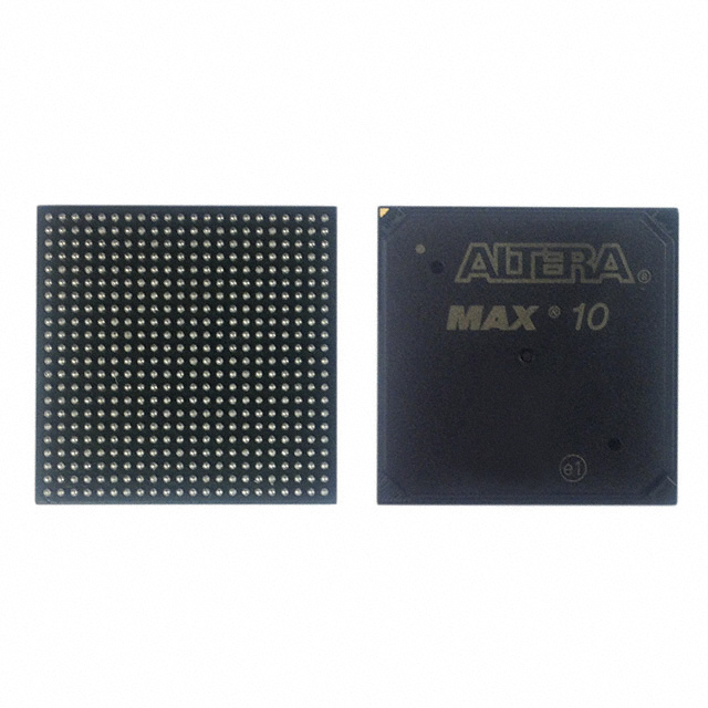
MAX® 10 Field Programmable Gate Array (FPGA) IC 250 387072 8000 484-BGA |
|---|---|
| Quantity | 1,035 Available (as of June 18, 2026) |

| Product Category | Field Programmable Gate Array (FPGA) |
|---|---|
| Manufacturer | Intel |
| Manufacturing Status | Active |
| Manufacturer Standard Lead Time | 16 Weeks |
| Datasheet |
Specifications & Environmental
| Device Package | 484-FBGA (23x23) | Grade | Industrial | Operating Temperature | -40°C – 100°C | ||
|---|---|---|---|---|---|---|---|
| Package / Case | 484-BGA | Number of I/O | 250 | Voltage | 1.15 V - 1.25 V | ||
| Mounting Method | Surface Mount | RoHS Compliance | RoHS non-compliant | REACH Compliance | REACH Affected | ||
| Moisture Sensitivity Level | 3 (168 Hours) | Number of LABs/CLBs | 500 | Number of Logic Elements/Cells | 8000 | ||
| Number of Gates | N/A | ECCN | 3A991A2 | HTS Code | 8542.31.0001 | ||
| Qualification | N/A | Total RAM Bits | 387072 |
Overview of 10M08DAF484I7P – MAX® 10 Field Programmable Gate Array (FPGA) IC 250 387072 8000 484-BGA
The 10M08DAF484I7P is a MAX® 10 field programmable gate array (FPGA) IC designed for applications that require configurable logic, on-chip RAM and a large number of general-purpose I/O. This device provides 8,000 logic elements, 387,072 bits of embedded RAM and up to 250 I/O pins in a compact 484-ball FBGA package.
With a supply voltage range of 1.15–1.25 V and an industrial-grade operating temperature range of −40 °C to 100 °C, the device targets designs that need moderate logic capacity, substantial on-chip memory and robust thermal performance.
Key Features
- Core Logic 8,000 logic elements for implementing custom digital functions and state machines.
- On-Chip Memory 387,072 bits of total RAM to support buffering, FIFOs and small data-storage requirements without external memory.
- I/O Density Up to 250 user I/O pins to support wide peripheral interfacing and parallel signal routing.
- Power Nominal voltage supply range of 1.15–1.25 V for core power planning and system integration.
- Package 484-ball FBGA (23 × 23 mm) package providing a high I/O count in a compact surface-mount footprint.
- Industrial Temperature Range Rated for operation from −40 °C to 100 °C for deployments in industrial and temperature-challenging environments.
- Mounting Surface-mount package suitable for automated PCB assembly workflows.
- RoHS Compliant Conforms to RoHS environmental requirements for lead-free assembly and regulatory compliance.
Typical Applications
- Industrial Control Implement control logic, sequencing and I/O aggregation where industrial temperature tolerance and reliability are required.
- Custom Logic Acceleration Offload application-specific processing or glue logic using the device’s 8,000 logic elements and extensive I/O.
- On-Board Memory and Buffering Use the 387,072 bits of embedded RAM for data buffering, small caches or packet FIFOs without adding external memory.
- I/O Expansion and Interface Bridging Leverage up to 250 I/O pins to consolidate multiple interfaces or provide wide parallel connections between subsystems.
Unique Advantages
- Balanced Logic and Memory: 8,000 logic elements paired with 387,072 bits of RAM supports a wide range of mid-density designs that need on-chip storage.
- High I/O Count in a Compact Package: 250 I/O pins within a 484-FBGA (23 × 23 mm) package maximize connectivity while minimizing PCB area.
- Industrial Temperature Qualification: Rated from −40 °C to 100 °C to meet the environmental demands of industrial applications.
- Controlled Core Voltage: A defined 1.15–1.25 V supply window simplifies power budgeting and core power sequencing.
- RoHS Compliant: Facilitates lead-free manufacturing and regulatory alignment for global production.
Why Choose 10M08DAF484I7P?
The 10M08DAF484I7P positions itself as a mid-density MAX® 10 FPGA option that combines a practical balance of logic capacity, substantial embedded RAM and a high I/O count in a compact 484-FBGA package. Its industrial temperature rating and controlled supply requirements make it suitable for designs where robustness and predictable power behavior are important.
This part is well-suited for engineers building industrial control systems, interface bridges, custom logic accelerators and embedded designs that require on-chip memory and dense I/O without moving to a larger footprint or external memory solutions. Selecting this device provides a clear specification set to plan power, thermal and PCB integration up front.
Request a quote or submit your pricing and availability inquiry today to evaluate the 10M08DAF484I7P for your next design.


Date Founded: 1968
Headquarters: Santa Clara, California, USA
Employees: 130,000+
Revenue: $54.23 Billion
Certifications and Memberships: ISO9001:2015, ISO14001:2015, ISO17025:2017, ISO27001:2022, ISO45001:2018, ISO50001:2018


