
10M08DCV81I7G
| Part Description |
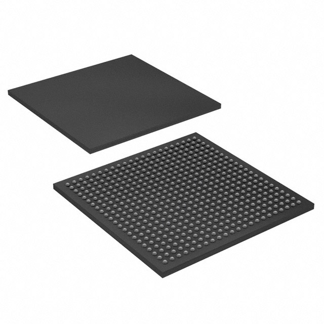
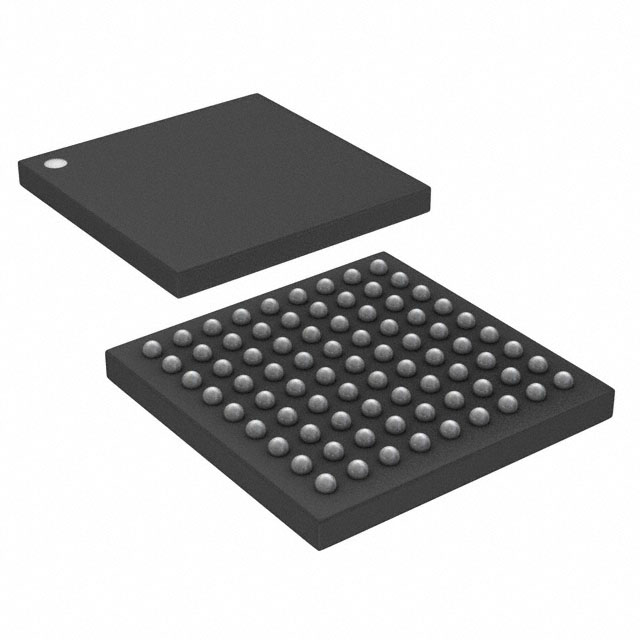
MAX® 10 Field Programmable Gate Array (FPGA) IC 56 387072 8000 81-UFBGA, WLCSP |
|---|---|
| Quantity | 324 Available (as of June 15, 2026) |

| Product Category | Field Programmable Gate Array (FPGA) |
|---|---|
| Manufacturer | Intel |
| Manufacturing Status | Active |
| Manufacturer Standard Lead Time | 16 Weeks |
| Datasheet |
Specifications & Environmental
| Device Package | 81-VBGA, WLCSP (4.5x4.4) | Grade | Industrial | Operating Temperature | -40°C – 100°C | ||
|---|---|---|---|---|---|---|---|
| Package / Case | 81-UFBGA, WLCSP | Number of I/O | 56 | Voltage | 1.15 V - 1.25 V | ||
| Mounting Method | Surface Mount | RoHS Compliance | RoHS Compliant | REACH Compliance | REACH Unaffected | ||
| Moisture Sensitivity Level | 1 (Unlimited) | Number of LABs/CLBs | 500 | Number of Logic Elements/Cells | 8000 | ||
| Number of Gates | N/A | ECCN | 3A991D | HTS Code | 8542.39.0001 | ||
| Qualification | N/A | Total RAM Bits | 387072 |
Overview of 10M08DCV81I7G – MAX® 10 FPGA, 8,000 Logic Elements, 56 I/O, 81‑UFBGA WLCSP
The 10M08DCV81I7G is an Intel MAX® 10 field programmable gate array (FPGA) device in an 81‑pin WLCSP package, specified for industrial-grade applications. It offers a compact, low‑voltage FPGA IC option with on‑chip RAM and a moderate logic capacity suitable for embedded control, signal interfacing, and industrial I/O functions.
Designed for deployment across industrial operating temperatures, this device provides a balance of integration and configurability with a 1.15 V–1.25 V supply range and RoHS compliance for regulatory compatibility.
Key Features
- Logic Capacity — 8,000 logic elements to implement custom logic, glue‑logic, and mid‑density FPGA functions.
- On‑chip Memory — 387,072 total RAM bits for FIFOs, buffering, and small data structures directly inside the device.
- I/O Capability — 56 I/O pins to connect sensors, actuators, buses, and peripheral devices within compact systems.
- Power — Core supply range 1.15 V to 1.25 V, enabling integration into low‑voltage power architectures.
- Package & Mounting — 81‑UFBGA / WLCSP package (supplier package listed as 81‑VBGA WLCSP, 4.5 × 4.4 mm); surface‑mount design for space‑constrained PCBs.
- Industrial Grade & Temperature Range — Specified operating temperature from −40 °C to 100 °C for industrial environments.
- Compliance — RoHS compliant for reduced hazardous substance content.
- Device Family & Speed Grades — Part of the Intel MAX 10 device family; MAX 10 device grades include industrial speed grades such as -I7 as referenced in the device series documentation.
Typical Applications
- Industrial Control — Use the 56 I/O and industrial temperature rating for machine control, supervisory logic, and I/O aggregation in industrial automation systems.
- Sensor and Actuator Interfaces — On‑chip RAM and moderate logic density enable local signal conditioning, filtering, and real‑time interfacing between sensors and controllers.
- Embedded Logic and Glue‑Code — Implement custom protocol bridging, timing logic, and peripheral management where a compact FPGA footprint is required.
Unique Advantages
- Right‑sized Logic Density: 8,000 logic elements provide a practical balance between capability and cost for mid‑range FPGA tasks without excess complexity.
- Substantial On‑chip RAM: 387,072 RAM bits reduce external memory needs for buffering and small data structures, simplifying BOM and board layout.
- Compact WLCSP Package: The 81‑pin WLCSP (4.5 × 4.4 mm supplier footprint) helps minimize board area for space‑limited designs.
- Industrial Temperature Range: −40 °C to 100 °C specification supports deployment in harsh or outdoor industrial environments.
- Low‑Voltage Core: 1.15 V–1.25 V supply requirement aligns with modern low‑voltage power rails and enables efficient power management.
- Regulatory Compliance: RoHS compliance supports adherence to environmental and regulatory requirements.
Why Choose 10M08DCV81I7G?
The 10M08DCV81I7G delivers a practical combination of logic resources, embedded RAM, and I/O density in a compact WLCSP package tailored for industrial applications. Its specified operating temperature range and low‑voltage core make it suitable for space‑constrained, ruggedized systems that require configurable logic without the footprint or power of larger FPGAs.
Choose this device when your design demands mid‑density programmable logic, local memory for buffering, and reliable operation across industrial temperatures—providing a scalable and verifiable building block for embedded control, I/O aggregation, and protocol bridging tasks.
If you would like pricing, availability, or a custom quote for 10M08DCV81I7G, submit a request today and our team will follow up with details and lead‑time information.


Date Founded: 1968
Headquarters: Santa Clara, California, USA
Employees: 130,000+
Revenue: $54.23 Billion
Certifications and Memberships: ISO9001:2015, ISO14001:2015, ISO17025:2017, ISO27001:2022, ISO45001:2018, ISO50001:2018


