
10M08DFV81C8GES
| Part Description |
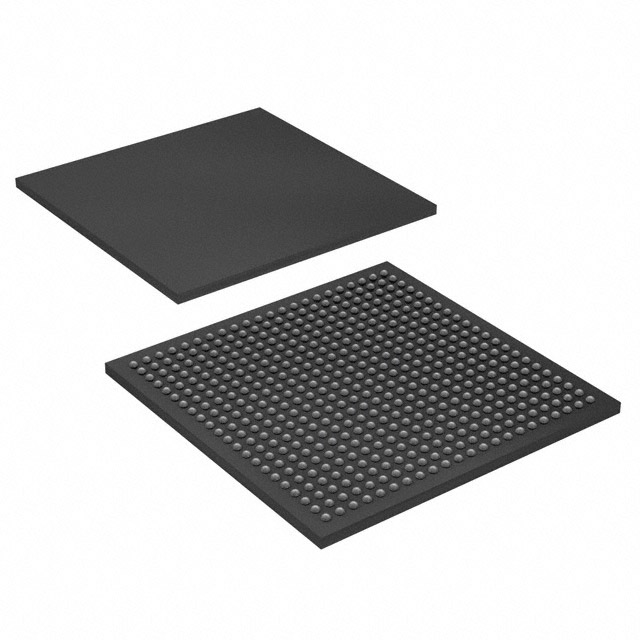
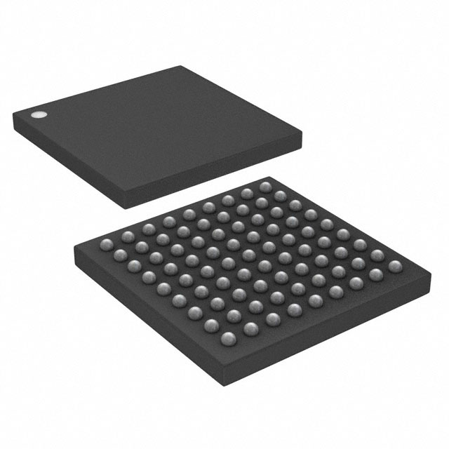
MAX® 10 Field Programmable Gate Array (FPGA) IC 56 387072 8000 81-UFBGA, WLCSP |
|---|---|
| Quantity | 122 Available (as of June 10, 2026) |

| Product Category | Field Programmable Gate Array (FPGA) |
|---|---|
| Manufacturer | Intel |
| Manufacturing Status | Discontinued |
| Manufacturer Standard Lead Time | 12 Weeks |
| Datasheet |
Specifications & Environmental
| Device Package | 81-VBGA, WLCSP (4.5x4.4) | Grade | Commercial | Operating Temperature | 0°C – 85°C | ||
|---|---|---|---|---|---|---|---|
| Package / Case | 81-UFBGA, WLCSP | Number of I/O | 56 | Voltage | 1.15 V - 1.25 V | ||
| Mounting Method | Surface Mount | RoHS Compliance | RoHS Compliant | REACH Compliance | REACH Unaffected | ||
| Moisture Sensitivity Level | 1 (Unlimited) | Number of LABs/CLBs | 500 | Number of Logic Elements/Cells | 8000 | ||
| Number of Gates | N/A | ECCN | 3A991D | HTS Code | 8542.39.0001 | ||
| Qualification | N/A | Total RAM Bits | 387072 |
Overview of 10M08DFV81C8GES – MAX® 10 FPGA, 8,000 Logic Elements, 387,072‑bit RAM, 56 I/O, 81‑UFBGA WLCSP
The 10M08DFV81C8GES is an Intel MAX® 10 field‑programmable gate array (FPGA) in a compact 81‑UFBGA WLCSP package. It provides on‑chip reconfigurable digital logic and embedded memory in a surface‑mount package for space‑constrained board designs.
Key device characteristics include approximately 8,000 logic elements, 387,072 total RAM bits, 56 user I/O, a core supply voltage range of 1.15 V to 1.25 V, and a commercial operating temperature range of 0 °C to 85 °C. The device is RoHS compliant and supplied in an 81‑VBGA WLCSP (4.5 × 4.4 mm) footprint.
Key Features
- Logic Capacity Approximately 8,000 logic elements for implementing custom digital logic and glue functions.
- Embedded Memory 387,072 total RAM bits of on‑chip memory to support buffers, FIFOs, and small data storage needs.
- I/O Resources 56 user I/O pins to interface with peripherals, sensors, and external devices.
- Power Core voltage range of 1.15 V to 1.25 V to match system power rails and aid power planning.
- Package & Mounting 81‑UFBGA, WLCSP package (supplier package 81‑VBGA WLCSP, 4.5 × 4.4 mm) designed for surface‑mount assembly in compact designs.
- Operating Conditions Commercial grade device rated for 0 °C to 85 °C operation.
- Environmental Compliance RoHS compliant for environmental and regulatory compatibility.
Typical Applications
- Embedded controllers Implement custom control logic and interface glue in compact embedded systems where on‑chip memory and a moderate number of I/Os are required.
- Protocol bridging Create custom protocol converters or bus bridges using the device's logic resources and I/O count for interfacing between subsystems.
- Prototyping and development Rapidly iterate digital designs and validate logic functions in a small, production‑aligned package.
- Consumer electronics Integrate custom control and timing functions in space‑restricted consumer products using the WLCSP footprint.
Unique Advantages
- Compact package density The 81‑UFBGA WLCSP (4.5 × 4.4 mm) package enables high functionality in a very small PCB area, reducing board footprint.
- Balanced logic and memory A combination of ~8,000 logic elements and 387,072 RAM bits supports mixed logic and buffering needs without external memory for many use cases.
- Moderate I/O count 56 I/Os provide flexibility to connect sensors, peripherals, and interfaces while keeping pin count and routing manageable.
- Defined power envelope A specified core supply range of 1.15 V to 1.25 V simplifies power supply design and integration into existing power architectures.
- Commercial temperature and compliance Rated for 0 °C to 85 °C operation and RoHS compliant for mainstream commercial product requirements.
Why Choose 10M08DFV81C8GES?
The 10M08DFV81C8GES delivers a practical balance of programmable logic, embedded memory, and I/O in a tiny WLCSP footprint. Its combination of ~8,000 logic elements, substantial on‑chip RAM, and 56 I/Os makes it well suited for compact board designs that require reconfigurable digital logic without large external components.
This commercial‑grade, RoHS‑compliant device is appropriate for customers seeking a compact, surface‑mount FPGA solution with clearly defined electrical and thermal ranges. It offers designers predictable supply requirements and package dimensions for efficient PCB layout and system integration.
Request a quote or submit an inquiry to get pricing and availability for 10M08DFV81C8GES. Include intended quantity and any delivery or packaging requirements for a tailored response.


Date Founded: 1968
Headquarters: Santa Clara, California, USA
Employees: 130,000+
Revenue: $54.23 Billion
Certifications and Memberships: ISO9001:2015, ISO14001:2015, ISO17025:2017, ISO27001:2022, ISO45001:2018, ISO50001:2018


