
10M08DFV81I7G
| Part Description |
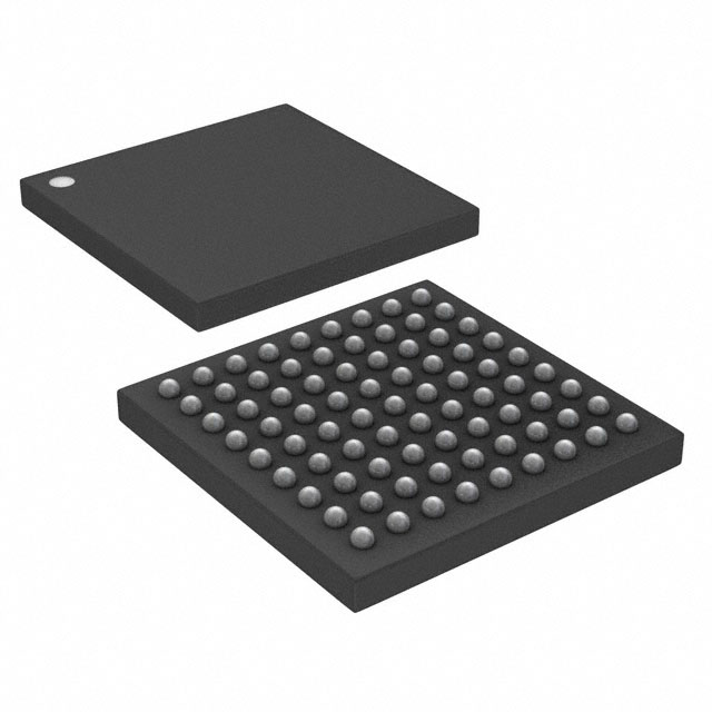
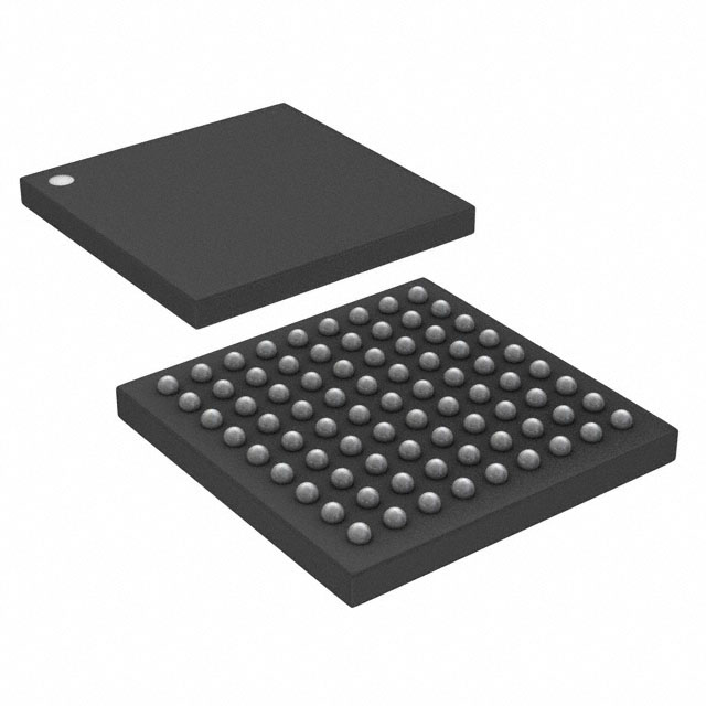
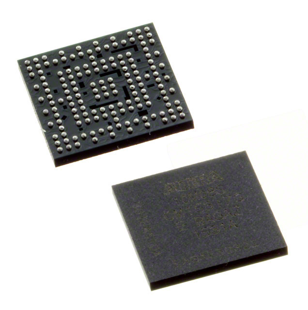
MAX® 10 Field Programmable Gate Array (FPGA) IC 56 387072 8000 81-UFBGA, WLCSP |
|---|---|
| Quantity | 439 Available (as of October 8, 2026) |
| Product Category | Field Programmable Gate Array (FPGA) |
|---|---|
| Manufacturer | Intel |
| Manufacturing Status | Active |
| Manufacturer Standard Lead Time | 16 Weeks |
| Datasheet |
Specifications & Environmental
| Device Package | 81-VBGA, WLCSP (4.5x4.4) | Grade | Industrial | Operating Temperature | -40°C – 100°C | ||
|---|---|---|---|---|---|---|---|
| Package / Case | 81-UFBGA, WLCSP | Number of I/O | 56 | Voltage | 1.15 V - 1.25 V | ||
| Mounting Method | Surface Mount | RoHS Compliance | RoHS Compliant | REACH Compliance | REACH Unaffected | ||
| Moisture Sensitivity Level | 1 (Unlimited) | Number of LABs/CLBs | 500 | Number of Logic Elements/Cells | 8000 | ||
| Number of Gates | N/A | ECCN | 3A991D | HTS Code | 8542.39.0001 | ||
| Qualification | N/A | Total RAM Bits | 387072 |
Overview of 10M08DFV81I7G – MAX® 10 FPGA, 8,000 logic elements, 56 I/Os
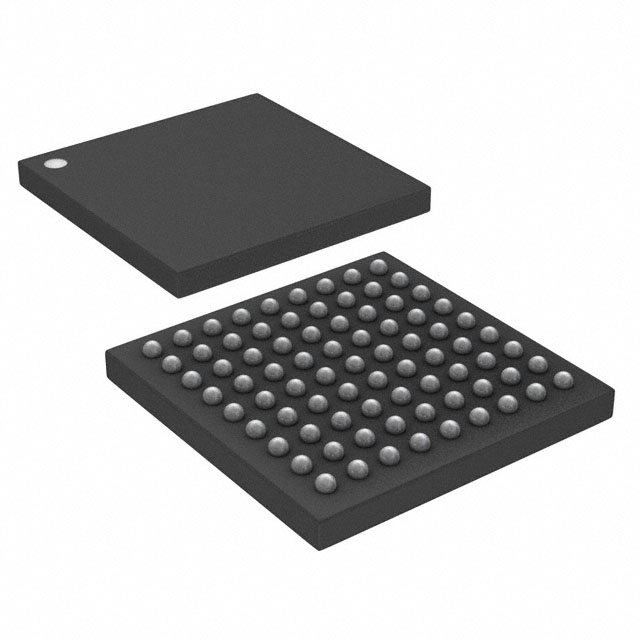
The 10M08DFV81I7G is an Intel MAX® 10 field programmable gate array (FPGA) supplied in an 81-UFBGA/WLCSP package. It delivers 8,000 logic elements and 387,072 bits of on‑chip RAM in a compact surface‑mount package with a 4.5×4.4 mm footprint.
Engineered as an industrial‑grade device, this FPGA supports a 1.15 V to 1.25 V supply range and an operating temperature range of −40 °C to 100 °C. The device datasheet provides detailed electrical, switching, configuration, and timing specifications for system design and integration.
Key Features
- Core Logic 8,000 logic elements for implementing combinational and sequential logic, state machines, and custom datapaths.
- On‑Chip Memory 387,072 total RAM bits to support buffering, lookup tables, and embedded state storage without external memory.
- I/O 56 available I/O pins to connect sensors, actuators, peripherals, and board-level interfaces.
- Power Supply Supported core voltage range of 1.15 V to 1.25 V for predictable power-rail design.
- Package & Mounting 81‑UFBGA (WLCSP) surface‑mount package; supplier device package listed as 81‑VBGA, WLCSP with a 4.5×4.4 mm footprint for space‑constrained layouts.
- Industrial Grade & Temperature Range Industrial grade device with an operating temperature range of −40 °C to 100 °C for extended environment applications.
- Documentation Comprehensive MAX 10 device datasheet covering electrical characteristics, switching characteristics, configuration specifications, and timing parameters to support system validation.
- RoHS Compliant Manufactured to RoHS environmental requirements.
Typical Applications
- Industrial Control Industrial‑grade operation and an extended temperature range make this FPGA suitable for control logic and interface tasks in automation equipment.
- Compact Embedded Systems Small WLCSP package (4.5×4.4 mm) and integrated logic/memory capacity support compact board designs where space is limited.
- Data Buffering & Processing On‑chip RAM (387,072 bits) combined with 8,000 logic elements supports local buffering, preprocessing, and finite state machines.
Unique Advantages
- High integration in a small footprint: 8,000 logic elements and substantial on‑chip RAM in an 81‑UFBGA/WLCSP package reduce the need for external components and conserve board area.
- Designed for industrial environments: Industrial grade rating and −40 °C to 100 °C operating range provide predictable operation across a wide range of ambient conditions.
- Predictable power requirements: Narrow supply window (1.15 V–1.25 V) helps simplify power‑rail design and margining for the FPGA core.
- Well‑documented device family: The MAX 10 FPGA datasheet includes electrical, switching, configuration, and timing details to support robust system integration and validation.
- RoHS compliance: Built to meet RoHS requirements for environmental compliance in manufacturing.
Why Choose 10M08DFV81I7G?
The 10M08DFV81I7G positions itself as a compact, industrial‑grade MAX 10 FPGA option that balances logic capacity, on‑chip memory, and I/O in a space‑efficient WLCSP package. Its defined core voltage range and extended operating temperature range make it suitable for engineers who need deterministic electrical and environmental characteristics.
This device is appropriate for designs that require moderate logic density and substantial on‑chip RAM in confined board real estate, supported by the MAX 10 device documentation for electrical, switching, and timing integration.
Request a quote or submit an inquiry to check availability and pricing for the 10M08DFV81I7G and begin integrating this MAX 10 FPGA into your next design.





















Date Founded: 1968
Headquarters: Santa Clara, California, USA
Employees: 130,000+
Revenue: $54.23 Billion
Certifications and Memberships: ISO9001:2015, ISO14001:2015, ISO17025:2017, ISO27001:2022, ISO45001:2018, ISO50001:2018


