
10M08DFV81C7G
| Part Description |
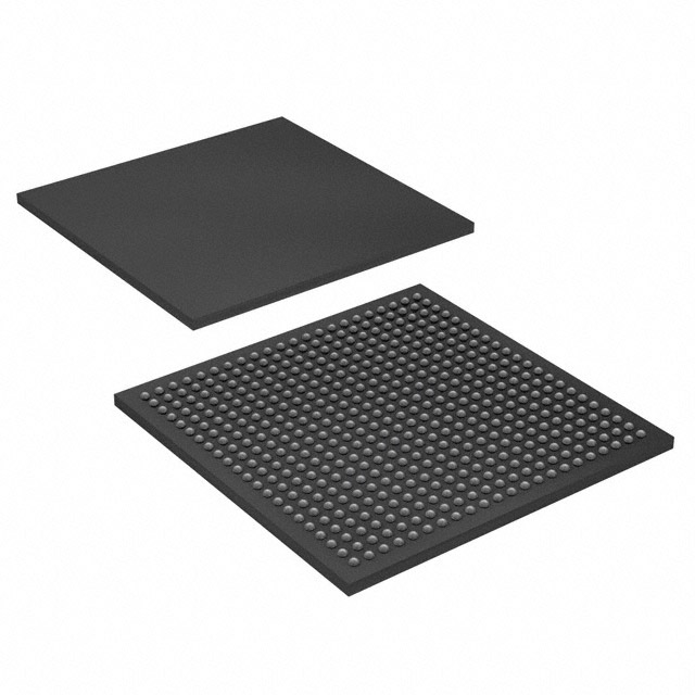
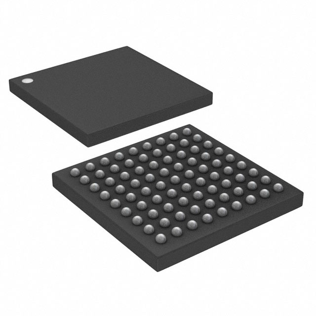
MAX® 10 Field Programmable Gate Array (FPGA) IC 56 387072 8000 81-UFBGA, WLCSP |
|---|---|
| Quantity | 1,027 Available (as of June 10, 2026) |

| Product Category | Field Programmable Gate Array (FPGA) |
|---|---|
| Manufacturer | Intel |
| Manufacturing Status | Active |
| Manufacturer Standard Lead Time | 16 Weeks |
| Datasheet |
Specifications & Environmental
| Device Package | 81-VBGA, WLCSP (4.5x4.4) | Grade | Commercial | Operating Temperature | 0°C – 85°C | ||
|---|---|---|---|---|---|---|---|
| Package / Case | 81-UFBGA, WLCSP | Number of I/O | 56 | Voltage | 1.15 V - 1.25 V | ||
| Mounting Method | Surface Mount | RoHS Compliance | RoHS Compliant | REACH Compliance | REACH Unaffected | ||
| Moisture Sensitivity Level | 1 (Unlimited) | Number of LABs/CLBs | 500 | Number of Logic Elements/Cells | 8000 | ||
| Number of Gates | N/A | ECCN | 3A991D | HTS Code | 8542.39.0001 | ||
| Qualification | N/A | Total RAM Bits | 387072 |
Overview of 10M08DFV81C7G – MAX® 10 FPGA IC, 8,000 logic elements, 387,072 RAM bits, 56 I/O, 81‑UFBGA WLCSP
The 10M08DFV81C7G is an Intel MAX® 10 field programmable gate array (FPGA) in a compact 81‑UFBGA WLCSP package. It delivers 8,000 logic elements, 387,072 bits of on-chip RAM, and 56 user I/O in a surface‑mount form factor targeted for commercial embedded designs.
Designed for space‑constrained, commercial applications, this device combines moderate logic capacity and on‑chip memory with a low‑voltage supply range and RoHS compliance for volume production use.
Key Features
- Logic Capacity — 8,000 logic elements to implement mid-density combinational and sequential logic.
- On‑chip Memory — 387,072 total RAM bits for data buffering, FIFOs, and small LUT-based storage structures.
- I/O — 56 user I/O pins to interface with peripherals, sensors, and external logic.
- Package & Mounting — 81‑UFBGA WLCSP package (supplier device package: 81‑VBGA WLCSP, 4.5 × 4.4 mm) optimized for surface‑mount, space‑limited PCBs.
- Power — Core supply range: 1.15 V to 1.25 V for integration into low‑voltage power domains.
- Operating Range — Commercial grade operation from 0 °C to 85 °C.
- Compliance — RoHS‑compliant for environmentally regulated manufacturing.
- Device Grade — Commercial grade device (part designation indicates commercial grade support).
Typical Applications
- Embedded control — Use the 8,000 logic elements and on‑chip RAM to implement custom control logic and finite state machines in commercial embedded products.
- I/O expansion and protocol bridging — 56 I/O pins provide flexible interfacing for bridging peripherals or adding custom interface logic to existing systems.
- Compact, board‑level integration — The 81‑UFBGA WLCSP (4.5 × 4.4 mm) package is suitable for space‑constrained PCB layouts where board area is limited.
- Production commercial systems — Commercial temperature range and RoHS compliance support standard commercial product qualification and manufacturing flows.
Unique Advantages
- Balanced logic and memory — 8,000 logic elements paired with 387,072 RAM bits provides a practical balance of LUT resources and on‑chip memory for many mid‑range designs.
- Compact WLCSP packaging — Small 81‑UFBGA WLCSP footprint (4.5 × 4.4 mm supplier dimension) enables high‑density board designs and reduces board area.
- Low‑voltage core operation — 1.15 V to 1.25 V supply range allows integration with modern low‑voltage power rails and optimized power delivery networks.
- Commercial production readiness — Commercial grade temperature range (0 °C to 85 °C) and RoHS compliance simplify qualification for mainstream commercial products.
- Surface‑mount convenience — Surface‑mount WLCSP package supports automated assembly and standard PCB manufacturing workflows.
Why Choose 10M08DFV81C7G?
The 10M08DFV81C7G positions itself as a compact, mid‑density FPGA option for commercial embedded designs that require a combination of logic capacity, on‑chip RAM, and a small WLCSP package. Its 8,000 logic elements, substantial RAM, and 56 I/O make it suitable for tasks such as control logic, interface bridging, and on‑board data buffering where board space and power are constrained.
For engineering teams targeting commercial product lines, this device offers a clear balance of integration, production readiness, and predictable operating conditions—helping reduce bill‑of‑materials complexity while enabling adaptable hardware logic in volume products.
Request a quote or submit an inquiry to obtain pricing, availability, and ordering information for the 10M08DFV81C7G.


Date Founded: 1968
Headquarters: Santa Clara, California, USA
Employees: 130,000+
Revenue: $54.23 Billion
Certifications and Memberships: ISO9001:2015, ISO14001:2015, ISO17025:2017, ISO27001:2022, ISO45001:2018, ISO50001:2018


