
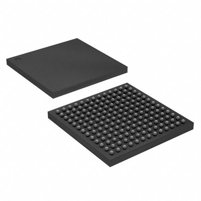
10M08SCU169C8G
| Part Description |
MAX® 10 Field Programmable Gate Array (FPGA) IC 130 387072 8000 169-LFBGA |
|---|---|
| Quantity | 390 Available (as of October 7, 2026) |
| Product Category | Field Programmable Gate Array (FPGA) |
|---|---|
| Manufacturer | Intel |
| Manufacturing Status | Active |
| Manufacturer Standard Lead Time | 12 Weeks |
| Datasheet |
Specifications & Environmental
| Device Package | 169-UBGA (11x11) | Grade | Commercial | Operating Temperature | 0°C – 85°C | ||
|---|---|---|---|---|---|---|---|
| Package / Case | 169-LFBGA | Number of I/O | 130 | Voltage | 2.85 V - 3.465 V | ||
| Mounting Method | Surface Mount | RoHS Compliance | RoHS Compliant | REACH Compliance | REACH Unaffected | ||
| Moisture Sensitivity Level | 3 (168 Hours) | Number of LABs/CLBs | 500 | Number of Logic Elements/Cells | 8000 | ||
| Number of Gates | N/A | ECCN | 3A991D | HTS Code | 8542.39.0001 | ||
| Qualification | N/A | Total RAM Bits | 387072 |
Overview of 10M08SCU169C8G – MAX® 10 Field Programmable Gate Array (FPGA) IC 130 387072 8000 169-LFBGA
The 10M08SCU169C8G is a commercial-grade MAX® 10 field programmable gate array (FPGA) from Intel, delivered in a 169-LFBGA package. It combines reprogrammable logic with on-chip RAM and a substantial I/O count to support compact, programmable designs.
With 8,000 logic elements, 387,072 bits of on-chip RAM and 130 I/O pins, this device targets commercial applications that require flexible digital logic, local data buffering and dense interfacing in a surface-mount form factor.
Key Features
- Core Logic 8,000 logic elements provide the reprogrammable fabric for implementing custom digital logic, state machines and control functions.
- Embedded Memory 387,072 total RAM bits supply on-chip storage for buffering, lookup tables and temporary data processing without external memory.
- High I/O Count 130 I/O pins enable broad connectivity for sensors, peripherals and parallel interfaces directly from the FPGA.
- Power Supply Supports a supply voltage range of 2.85 V to 3.465 V to match common commercial power rails.
- Package and Mounting 169-LFBGA package (supplier package: 169-UBGA 11×11) in a surface-mount format for compact board-level integration.
- Operating Range and Grade Commercial grade with an operating temperature range of 0°C to 85°C suitable for standard commercial-environment applications.
- Environmental Compliance RoHS compliant to meet common environmental and manufacturing requirements.
Typical Applications
- Embedded Control and Automation 8,000 logic elements and 130 I/Os enable implementation of control logic, peripheral interfaces and sensor management in commercial devices.
- Data Buffering and Stream Handling 387,072 bits of on-chip RAM provide local buffering and temporary storage for streaming data and packet staging without immediate external memory.
- Protocol Bridging and Custom I/O The high I/O count supports protocol adaptation, bus bridging and glue logic between heterogeneous subsystems.
- Compact System Integration The 169-LFBGA surface-mount package suits space-constrained designs where board area and component density matter.
Unique Advantages
- Reprogrammable Logic Capacity: 8,000 logic elements let you iterate hardware functions in-system and implement custom digital architectures without redesigning PCBs.
- Substantial On-Chip RAM: 387,072 bits of memory reduce reliance on external RAM for many buffering and temporary storage needs, simplifying BOM and layout.
- Flexible Connectivity: 130 I/O pins provide headroom for direct connections to peripherals, sensors and user interfaces, reducing the need for GPIO expanders.
- Commercial-Grade Operating Range: Rated 0°C to 85°C for typical commercial environments where consistent operation in that range is required.
- Compact Surface-Mount Package: 169-LFBGA (169-UBGA 11×11) supports dense board layouts and automated assembly processes.
- RoHS Compliant: Meets common environmental compliance requirements for modern electronics manufacturing.
Why Choose 10M08SCU169C8G?
The 10M08SCU169C8G positions itself as a versatile commercial-grade FPGA that balances logic capacity, on-chip memory and I/O density in a compact LFBGA package. It is well suited for engineers designing commercial embedded systems that need programmable logic, local data storage and flexible interfacing without adding external memory or large board area.
Choose this device when your design requires a reprogrammable, integrated solution with clear electrical and thermal bounds (2.85 V–3.465 V, 0°C–85°C) and RoHS compliance for streamlined manufacturing and procurement.
Request a quote or submit an inquiry to get pricing and availability information for the 10M08SCU169C8G.
























Date Founded: 1968
Headquarters: Santa Clara, California, USA
Employees: 130,000+
Revenue: $54.23 Billion
Certifications and Memberships: ISO9001:2015, ISO14001:2015, ISO17025:2017, ISO27001:2022, ISO45001:2018, ISO50001:2018


