
10M08SFE144C7G
| Part Description |
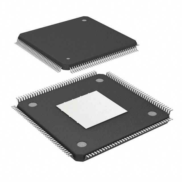
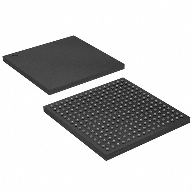
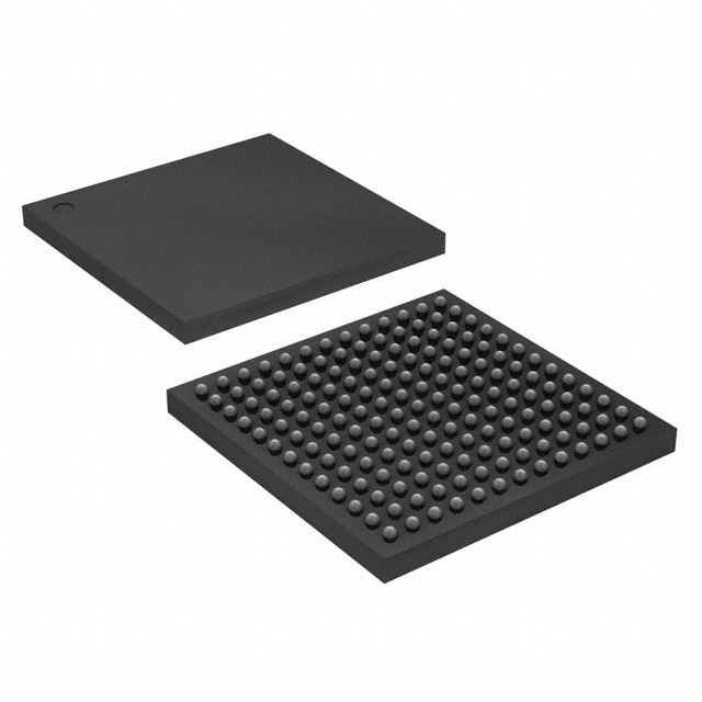
MAX® 10 Field Programmable Gate Array (FPGA) IC 101 387072 8000 144-LQFP Exposed Pad |
|---|---|
| Quantity | 147 Available (as of October 8, 2026) |
| Product Category | Field Programmable Gate Array (FPGA) |
|---|---|
| Manufacturer | Intel |
| Manufacturing Status | Obsolete |
| Manufacturer Standard Lead Time | Contact Us |
| Datasheet |
Specifications & Environmental
| Device Package | 144-EQFP (20x20) | Grade | Commercial | Operating Temperature | 0°C – 85°C | ||
|---|---|---|---|---|---|---|---|
| Package / Case | 144-LQFP Exposed Pad | Number of I/O | 101 | Voltage | 2.85 V - 3.465 V | ||
| Mounting Method | Surface Mount | RoHS Compliance | Unknown | REACH Compliance | REACH Unaffected | ||
| Moisture Sensitivity Level | 3 (168 Hours) | Number of LABs/CLBs | 500 | Number of Logic Elements/Cells | 8000 | ||
| Number of Gates | N/A | ECCN | 3A991D | HTS Code | 8542.39.0001 | ||
| Qualification | N/A | Total RAM Bits | 387072 |
Overview of 10M08SFE144C7G – MAX® 10 FPGA, 8,000 logic elements, 101 I/O
The 10M08SFE144C7G is a MAX® 10 Field Programmable Gate Array (FPGA) IC from Intel in a 144-LQFP exposed pad package. It integrates 8,000 logic elements, 387,072 bits of RAM and 101 general-purpose I/O to address mid-range programmable-logic requirements.
Designed for commercial-grade applications, this device supports a 2.85 V to 3.465 V supply range and operates from 0 °C to 85 °C, offering a balanced combination of logic capacity, on-chip memory, and I/O density for embedded designs and system-level integration.
Key Features
- Core Logic 8,000 logic elements provide the programmable logic capacity needed for mid-range integration and custom hardware acceleration.
- Logic Structure 500 LABs/CLBs (as specified) to organize logic resources for structured design implementation.
- On-Chip Memory 387,072 total RAM bits for data buffering, FIFOs, and small memory blocks directly within the FPGA fabric.
- I/O Density 101 I/O pins to support multiple parallel interfaces, board-level connectivity, and peripheral integration.
- Power Voltage supply range of 2.85 V to 3.465 V to support common system power rails.
- Package 144-LQFP exposed pad (supplier device package: 144-EQFP 20×20) for surface-mount PCB assembly and thermal dissipation through the exposed pad.
- Operating Range Commercial operating temperature range from 0 °C to 85 °C.
- Compliance RoHS compliant.
Typical Applications
- Logic-dense designs Systems that require up to 8,000 logic elements and organized LAB/CLB resources for custom digital functions.
- I/O-heavy interfaces Designs needing 101 general-purpose I/O pins for board-level peripherals, parallel buses, or multiple interfaces.
- On-chip memory usage Applications that leverage 387,072 bits of RAM for buffering, small memories, or data-path storage within the FPGA fabric.
- Commercial embedded systems Projects operating within a 0 °C to 85 °C temperature window and using standard 2.85 V–3.465 V supply rails.
Unique Advantages
- Balanced logic and memory combination: 8,000 logic elements paired with 387,072 bits of RAM enable integrated implementation of control, data-path, and buffering functions on a single device.
- High I/O capacity: 101 I/O pins support multiple external interfaces without immediate need for I/O expanders, simplifying board-level design.
- Commercial-grade thermal and power compatibility: The device’s operating range (0 °C to 85 °C) and 2.85 V–3.465 V supply compatibility align with typical commercial embedded power systems.
- Surface-mount exposed pad package: 144-LQFP with exposed pad provides PCB-friendly mounting and an opportunity for improved thermal performance through the pad.
- Regulatory-friendly supply chain: RoHS compliance supports lead-free manufacturing requirements.
Why Choose 10M08SFE144C7G?
The 10M08SFE144C7G positions itself as a practical mid-range FPGA option that combines substantial logic capacity, meaningful on-chip RAM, and generous I/O resources in a compact 144-LQFP exposed pad package. Its electrical and thermal specifications make it suitable for commercial embedded systems that require integrated logic and memory without moving to larger device families.
Engineers and procurement teams seeking a field-programmable device with clear, verifiable specifications—8,000 logic elements, 387,072 RAM bits, 101 I/O, RoHS compliance, and a 0 °C to 85 °C operating window—will find this part suitable for scalable designs and predictable integration into existing supply chains.
If you would like pricing or availability, request a quote or submit a quote request and our team will respond with current lead times and ordering options.





















Date Founded: 1968
Headquarters: Santa Clara, California, USA
Employees: 130,000+
Revenue: $54.23 Billion
Certifications and Memberships: ISO9001:2015, ISO14001:2015, ISO17025:2017, ISO27001:2022, ISO45001:2018, ISO50001:2018


