
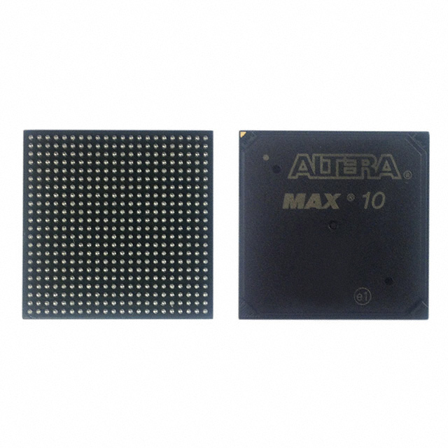
10M08SCU324I7G
| Part Description |
MAX® 10 Field Programmable Gate Array (FPGA) IC 246 387072 8000 324-LFBGA |
|---|---|
| Quantity | 1,420 Available (as of June 15, 2026) |

| Product Category | Field Programmable Gate Array (FPGA) |
|---|---|
| Manufacturer | Intel |
| Manufacturing Status | Active |
| Manufacturer Standard Lead Time | 12 Weeks |
| Datasheet |
Specifications & Environmental
| Device Package | 324-UBGA (15x15) | Grade | Industrial | Operating Temperature | -40°C – 100°C | ||
|---|---|---|---|---|---|---|---|
| Package / Case | 324-LFBGA | Number of I/O | 246 | Voltage | 1.15 V - 1.25 V | ||
| Mounting Method | Surface Mount | RoHS Compliance | Unknown | REACH Compliance | REACH Unknown | ||
| Moisture Sensitivity Level | 3 (168 Hours) | Number of LABs/CLBs | 500 | Number of Logic Elements/Cells | 8000 | ||
| Number of Gates | N/A | ECCN | N/A | HTS Code | 8542.39.0001 | ||
| Qualification | N/A | Total RAM Bits | 387072 |
Overview of 10M08SCU324I7G – MAX® 10 FPGA, 8,000 logic elements, 387,072 RAM bits, 246 I/O, 324-LFBGA
The 10M08SCU324I7G is an Intel MAX® 10 field programmable gate array (FPGA) offered in a 324-ball LFBGA package. It provides reprogrammable digital logic with 8,000 logic elements and on-chip RAM totaling 387,072 bits, making it suitable for embedded and industrial designs that require flexible, board-level programmable logic.
Designed and specified for industrial operation, this 10M08 device supports a -I7 speed grade and delivers a balance of logic capacity, on-chip memory, and high pin-count I/O for applications that need moderate logic density and extensive external connectivity.
Key Features
- Core Logic 8,000 logic elements provide the programmable fabric for custom logic, state machines, and control functions.
- Logic Array Blocks 500 logic array blocks (LABs) for organized placement of logic resources and predictable partitioning.
- On-chip Memory 387,072 total RAM bits to support buffering, FIFOs, and small embedded data stores without external memory.
- I/O Capacity 246 general-purpose I/O pins for broad interfacing to sensors, buses, and peripherals.
- Power Supply Core voltage support from 1.15 V to 1.25 V to match system power budgets and regulator designs.
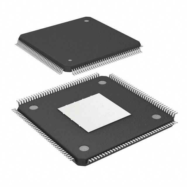
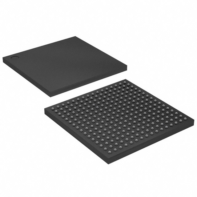
- Package & Mounting 324-LFBGA package (supplier device package: 324-UBGA, 15×15) in a surface-mount form factor for compact board designs.
- Operating Range Industrial temperature rating from −40 °C to 100 °C for deployment in temperature-demanding environments.
- Compliance RoHS-compliant construction for regulatory and environmental conformity.
Typical Applications
- Industrial Control Use the 10M08SCU324I7G to implement deterministic control logic and I/O aggregation where the −40 °C to 100 °C rating and 246 I/O pins support robust sensor and actuator interfacing.
- Embedded System Customization Implement custom glue logic, protocol bridging, or preprocessing functions using 8,000 logic elements and on-chip RAM to reduce external components.
- High‑Pin‑Count I/O Expansion Leverage the 246 I/O pins in systems that require dense peripheral connections or multiple parallel interfaces while keeping the design compact with the 324-LFBGA package.
Unique Advantages
- Balanced logic and memory: 8,000 logic elements paired with 387,072 RAM bits allow meaningful on‑chip implementation of stateful logic and buffering without immediate need for external memory.
- High I/O density: 246 I/O pins provide flexibility for complex interfacing, reducing the need for external I/O expanders.
- Industrial temperature capability: Rated from −40 °C to 100 °C to meet environmental requirements for many industrial applications.
- Compact surface-mount package: The 324-LFBGA (324-UBGA, 15×15) footprint supports space-constrained PCBs while delivering substantial I/O and logic resources.
- Low-voltage core: 1.15 V to 1.25 V core supply allows integration into systems with modern low-voltage power rails.
- Regulatory compliance: RoHS compliance simplifies end‑product regulatory planning.
Why Choose 10M08SCU324I7G?
The 10M08SCU324I7G positions itself as a versatile, industrial‑grade MAX® 10 FPGA option for designs that require moderate logic density, substantial on‑chip RAM, and high I/O count in a compact surface‑mount package. Its −40 °C to 100 °C operating range and -I7 speed grade make it appropriate for applications that demand reliable operation across a wide temperature span.
Engineers and procurement teams seeking a reprogrammable, RoHS-compliant FPGA with clear electrical and mechanical parameters will find this device suitable for embedded control, I/O consolidation, and system customization tasks where integration and predictable specs matter.
Request a quote or submit a product inquiry today to evaluate the 10M08SCU324I7G for your next design.


Date Founded: 1968
Headquarters: Santa Clara, California, USA
Employees: 130,000+
Revenue: $54.23 Billion
Certifications and Memberships: ISO9001:2015, ISO14001:2015, ISO17025:2017, ISO27001:2022, ISO45001:2018, ISO50001:2018


