
10M40DCF256C7G
| Part Description |
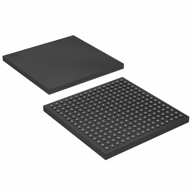
MAX® 10 Field Programmable Gate Array (FPGA) IC 178 1290240 40000 256-LBGA |
|---|---|
| Quantity | 876 Available (as of October 8, 2026) |
| Product Category | Field Programmable Gate Array (FPGA) |
|---|---|
| Manufacturer | Intel |
| Manufacturing Status | Active |
| Manufacturer Standard Lead Time | 16 Weeks |
| Datasheet |
Specifications & Environmental
| Device Package | 256-FBGA (17x17) | Grade | Commercial | Operating Temperature | 0°C – 85°C | ||
|---|---|---|---|---|---|---|---|
| Package / Case | 256-LBGA | Number of I/O | 178 | Voltage | 1.15 V - 1.25 V | ||
| Mounting Method | Surface Mount | RoHS Compliance | RoHS Compliant | REACH Compliance | REACH Unaffected | ||
| Moisture Sensitivity Level | 3 (168 Hours) | Number of LABs/CLBs | 2500 | Number of Logic Elements/Cells | 40000 | ||
| Number of Gates | N/A | ECCN | 3A991D | HTS Code | 8542.39.0001 | ||
| Qualification | N/A | Total RAM Bits | 1290240 |
Overview of 10M40DCF256C7G – MAX® 10 FPGA, 40,000 logic elements, 1,290,240-bit RAM, 256-LBGA
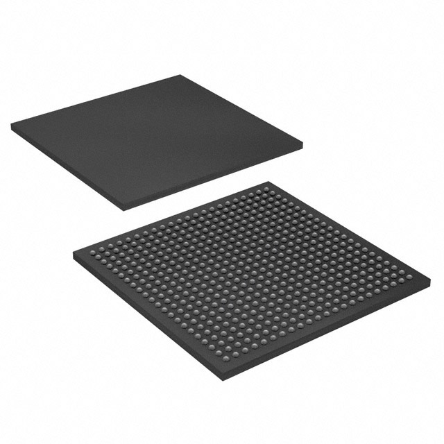
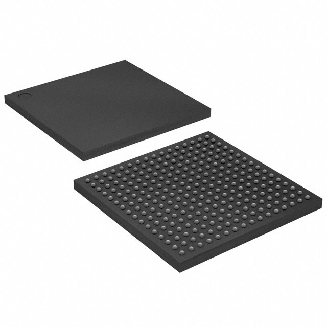
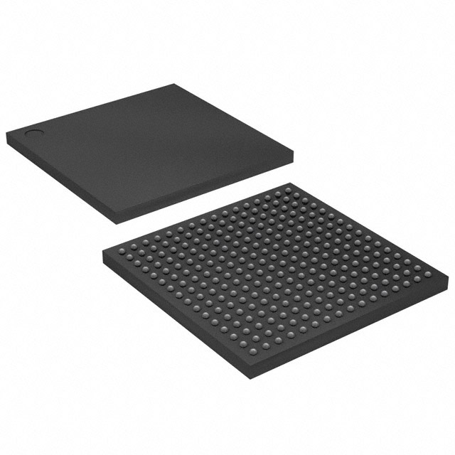
The 10M40DCF256C7G is an Intel MAX® 10 field-programmable gate array (FPGA) provided in a 256-ball LBGA package. It delivers a high-density programmable fabric with 40,000 logic elements and 1,290,240 bits of on-chip RAM for compact, configurable digital designs.
Designed for commercial applications, this device combines a large logic capacity, extensive I/O (178 pins), and a documented set of electrical, switching, and configuration specifications to support system integration and development workflows.
Key Features
- Logic Capacity 40,000 logic elements support complex custom logic, state machines, and control functions.
- On‑Chip Memory 1,290,240 total RAM bits provide embedded storage for buffering, FIFOs, and small lookup tables.
- I/O Density 178 I/O pins enable broad interfacing to peripherals, sensors, and external logic domains.
- Core Supply Operates from a 1.15 V to 1.25 V core supply as specified for this device.
- Package & Mounting 256-LBGA package (supplier package: 256-FBGA, 17 × 17 mm) with surface-mount mounting suitable for compact board layouts.
- Commercial Grade & Temperature Commercial grade device with an operating temperature range of 0 °C to 85 °C.
- Configuration & Timing Documentation Datasheet provides electrical characteristics, switching characteristics, configuration specifications, JTAG timing, and related timing information to support design and verification.
- Environmental Compliance RoHS compliant.
Typical Applications
- Custom Digital Logic & Prototyping Use the programmable fabric and on-chip RAM to prototype and iterate digital subsystems and IP blocks.
- Commercial Embedded Systems Implement control, glue logic, and protocol bridging in compact, commercial-grade products.
- I/O Aggregation & Interface Bridging Leverage 178 I/O pins to aggregate signals and bridge between multiple peripherals or buses.
- User Interface & Peripheral Control Deploy logic and RAM for driving displays, handling input scanning, and managing peripheral timing.
Unique Advantages
- High Logic Density: 40,000 logic elements enable substantial on-chip implementation of complex logic without external ASICs.
- Significant Embedded RAM: 1,290,240 bits of RAM reduce the need for external memory in many buffering and storage tasks.
- Extensive I/O Count: 178 I/Os provide flexibility for multi-peripheral and multi-protocol designs on a single device.
- Compact Package: 256-LBGA / 256-FBGA (17×17 mm) package supports dense PCB layouts while maintaining surface-mount assembly.
- Commercial Temperature & Supply Range: Operates across a 0 °C to 85 °C range with a defined 1.15 V–1.25 V core supply for predictable integration into commercial systems.
- Documented Electrical & Configuration Data: Comprehensive datasheet coverage of electrical characteristics, switching, and configuration timing aids design verification and risk reduction.
Why Choose 10M40DCF256C7G?
The 10M40DCF256C7G brings together a large logic fabric, abundant on‑chip RAM, and a high I/O count in a compact surface-mount package tailored for commercial embedded designs. Its documented electrical and configuration specifications help accelerate integration, verification, and production readiness for designs requiring configurable logic and interfacing capability.
This device suits engineers and procurement teams seeking a scalable, documented FPGA building block for custom logic, I/O aggregation, and embedded control tasks where a commercial-grade, RoHS-compliant solution is required.
Request a quote or submit an inquiry to obtain pricing and availability for the 10M40DCF256C7G.























Date Founded: 1968
Headquarters: Santa Clara, California, USA
Employees: 130,000+
Revenue: $54.23 Billion
Certifications and Memberships: ISO9001:2015, ISO14001:2015, ISO17025:2017, ISO27001:2022, ISO45001:2018, ISO50001:2018


