
10M40SCE144C7G
| Part Description |
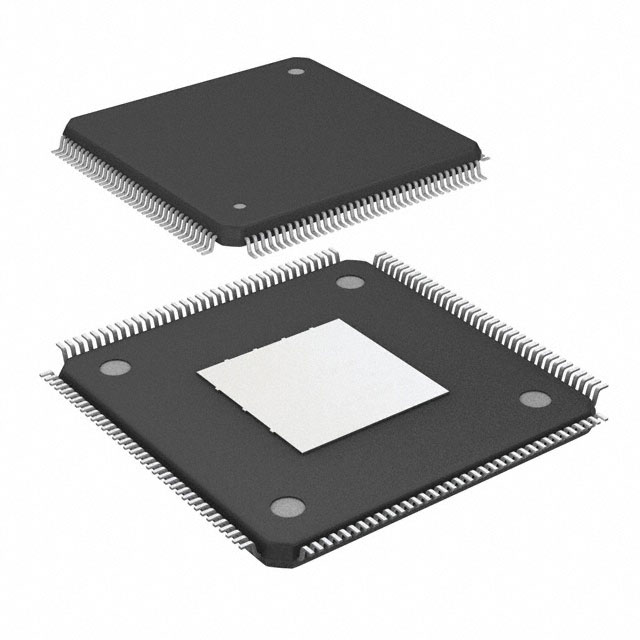
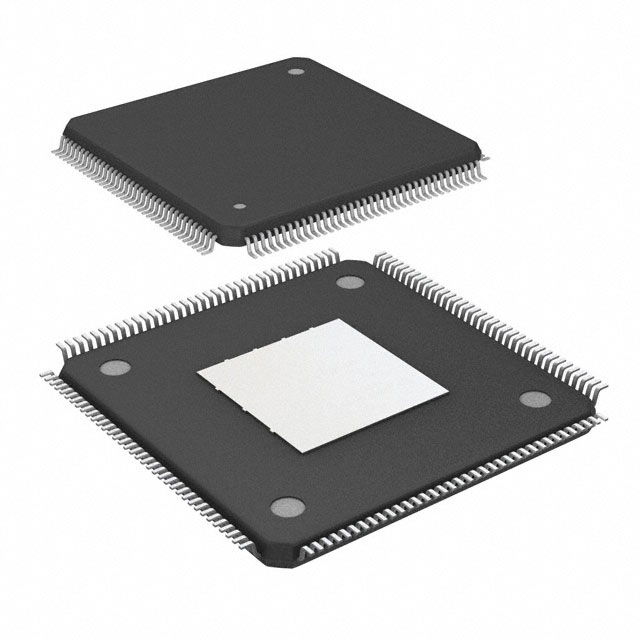
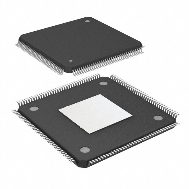
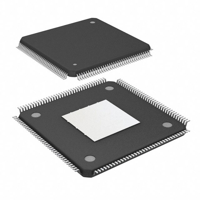
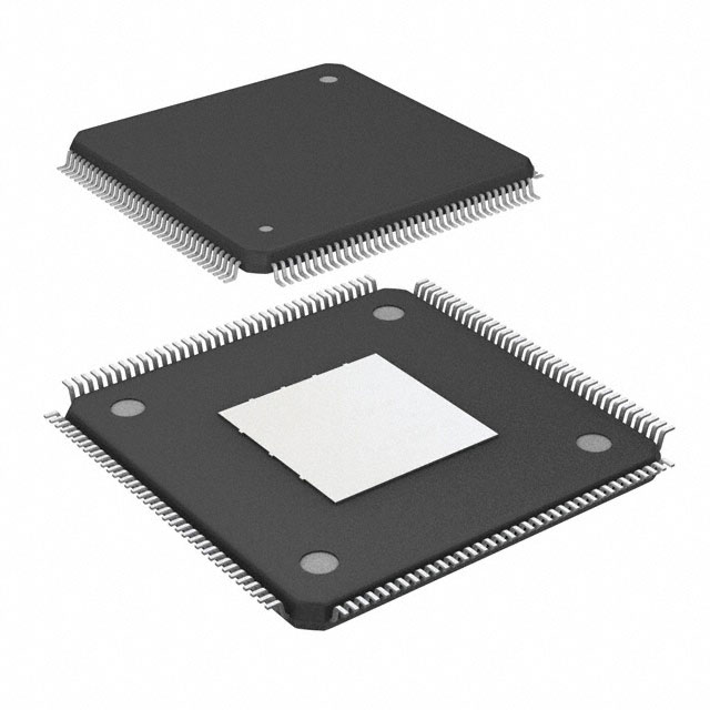
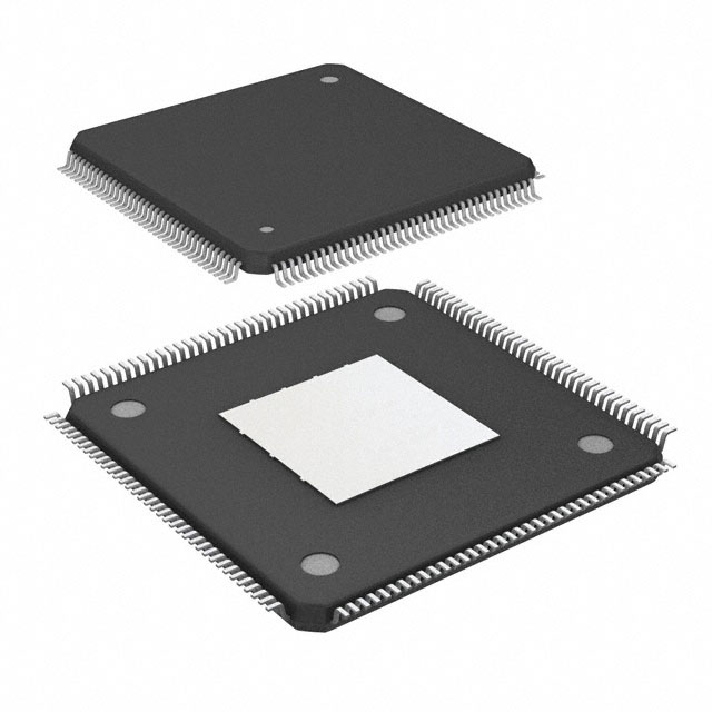
MAX® 10 Field Programmable Gate Array (FPGA) IC 101 1290240 40000 144-LQFP Exposed Pad |
|---|---|
| Quantity | 367 Available (as of October 7, 2026) |
| Product Category | Field Programmable Gate Array (FPGA) |
|---|---|
| Manufacturer | Intel |
| Manufacturing Status | Obsolete |
| Manufacturer Standard Lead Time | Contact Us |
| Datasheet |
Specifications & Environmental
| Device Package | 144-EQFP (20x20) | Grade | Commercial | Operating Temperature | 0°C – 85°C | ||
|---|---|---|---|---|---|---|---|
| Package / Case | 144-LQFP Exposed Pad | Number of I/O | 101 | Voltage | 2.85 V - 3.465 V | ||
| Mounting Method | Surface Mount | RoHS Compliance | Unknown | REACH Compliance | REACH Unaffected | ||
| Moisture Sensitivity Level | 3 (168 Hours) | Number of LABs/CLBs | 2500 | Number of Logic Elements/Cells | 40000 | ||
| Number of Gates | N/A | ECCN | 3A991D | HTS Code | 8542.39.0001 | ||
| Qualification | N/A | Total RAM Bits | 1290240 |
Overview of 10M40SCE144C7G – MAX® 10 FPGA, 101 I/Os, 40,000 Logic Elements, 1,290,240 RAM Bits, 144-LQFP
The 10M40SCE144C7G is an Intel MAX® 10 field programmable gate array (FPGA) supplied in a 144-LQFP exposed-pad package. It combines a high density of programmable logic with substantial on-chip RAM and a moderate I/O count for versatile board-level integration.
Designed for surface-mount assembly and commercial-grade operation, this device supports a 2.85 V to 3.465 V supply range and an operating temperature range of 0 °C to 85 °C, making it suitable for a broad set of general-purpose embedded and digital logic designs that require reprogrammable hardware resources.
Key Features
- Logic Density: 40,000 logic elements provide the capacity to implement medium-complexity digital designs and custom logic functions.
- Logic Blocks (CLBs/LABs): 2,500 logic blocks support structured placement of logic resources for efficient utilization of the device fabric.
- On‑Chip Memory: 1,290,240 total RAM bits enable local buffering, lookup-tables, and state storage without external memory.
- I/O Count: 101 I/Os available for interfacing with peripherals, sensors, and external logic on the PCB.
- Power Supply Range: Operates from 2.85 V to 3.465 V, accommodating common board-level power rails.
- Package & Mounting: 144-LQFP exposed pad (supplier package: 144-EQFP, 20×20) in a surface-mount configuration for compact PCB designs and thermal stability through the exposed pad.
- Temperature Grade: Commercial operating range from 0 °C to 85 °C for standard ambient applications.
- Compliance: RoHS compliant, meeting lead-free environmental requirements.
Typical Applications
- Custom Logic and Prototyping: Implement application-specific digital functions and iterate designs using the device's programmable logic and on-chip memory.
- I/O Expansion and Protocol Bridging: Use the 101 I/Os to bridge and translate between multiple interfaces or to expand MCU/processor connectivity on a single board.
- Data Buffering and Preprocessing: Leverage the 1,290,240 bits of RAM for local buffering, FIFO implementations, and real-time preprocessing of data streams.
Unique Advantages
- Balanced Resource Mix: Combines 40,000 logic elements with over 1.29 Mbit of RAM to address designs needing both combinational logic and local memory.
- Compact, Thermally Managed Package: The 144-LQFP exposed pad layout supports surface-mount assembly while providing a thermal path for heat dissipation on populated PCBs.
- Flexible I/O Count: 101 I/Os let you connect a variety of peripherals and external devices without immediate need for extra I/O expanders.
- Standard Commercial Grade: Rated for 0 °C to 85 °C operation and RoHS compliant, suitable for mainstream commercial and embedded applications.
- Wide Supply Compatibility: Operates across a 2.85 V to 3.465 V supply range, aligning with common board power architectures.
Why Choose 10M40SCE144C7G?
The 10M40SCE144C7G positions itself as a practical, mid-density FPGA option that pairs a substantial logic element count and large on-chip RAM with a flexible I/O complement in a board-friendly 144-LQFP exposed-pad package. Its commercial temperature rating and RoHS compliance make it a reliable choice for general-purpose embedded designs that require reprogrammable hardware capability without the complexity of higher-end families.
This device is well suited to design teams seeking a scalable, on-board programmable solution for custom logic, data buffering, and interface bridging, delivering long-term value through reprogrammability and a focused set of integrated resources.
Request a quote or submit a pricing inquiry to get current availability, lead time, and volume pricing for the 10M40SCE144C7G. Our team can provide the details you need to move your design forward.





















Date Founded: 1968
Headquarters: Santa Clara, California, USA
Employees: 130,000+
Revenue: $54.23 Billion
Certifications and Memberships: ISO9001:2015, ISO14001:2015, ISO17025:2017, ISO27001:2022, ISO45001:2018, ISO50001:2018


