
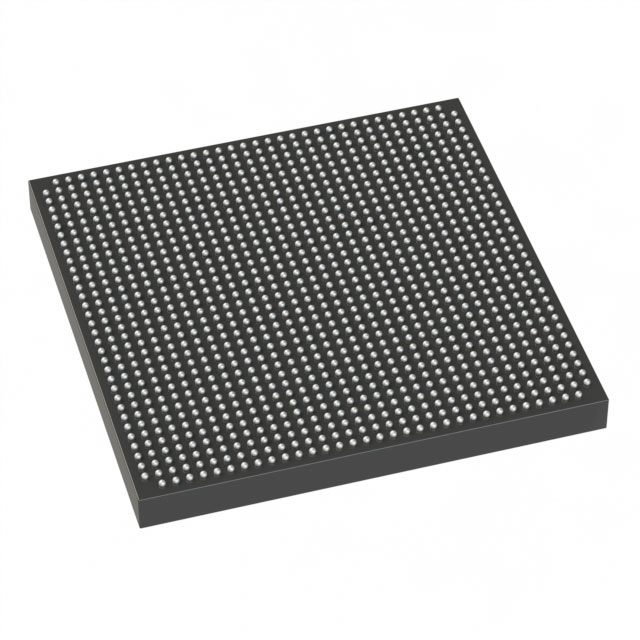
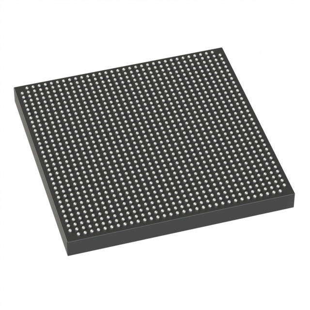
1SG065HH2F35E2VG
| Part Description |
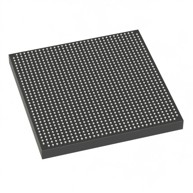
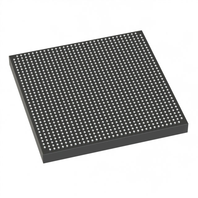
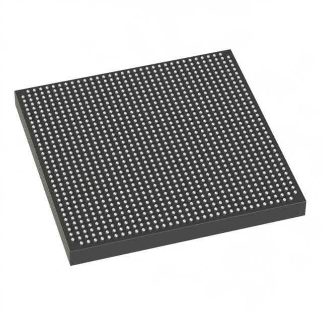
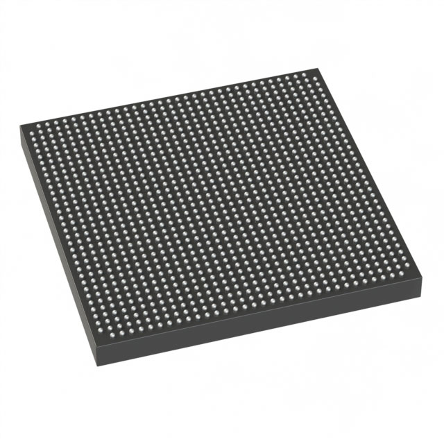
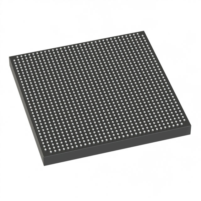
Stratix® 10 GX Field Programmable Gate Array (FPGA) IC 392 51380224 612000 1152-BBGA, FCBGA |
|---|---|
| Quantity | 677 Available (as of October 8, 2026) |
| Product Category | Field Programmable Gate Array (FPGA) |
|---|---|
| Manufacturer | Intel |
| Manufacturing Status | Active |
| Manufacturer Standard Lead Time | 12 Weeks |
| Datasheet |
Specifications & Environmental
| Device Package | 1152-FBGA (35x35) | Grade | Extended | Operating Temperature | 0°C – 100°C | ||
|---|---|---|---|---|---|---|---|
| Package / Case | 1152-BBGA, FCBGA | Number of I/O | 392 | Voltage | 770 mV - 970 mV | ||
| Mounting Method | Surface Mount | RoHS Compliance | Unknown | REACH Compliance | REACH Unknown | ||
| Moisture Sensitivity Level | 3 (168 Hours) | Number of LABs/CLBs | 76500 | Number of Logic Elements/Cells | 612000 | ||
| Number of Gates | N/A | ECCN | N/A | HTS Code | N/A | ||
| Qualification | N/A | Total RAM Bits | 51380224 |
Overview of 1SG065HH2F35E2VG – Stratix® 10 GX Field Programmable Gate Array (FPGA)
The 1SG065HH2F35E2VG is an Intel Stratix® 10 GX FPGA provided in a 1152‑BBGA (FCBGA) surface‑mount package. It delivers a large logic fabric and on‑chip memory capacity intended for designs that require significant programmable logic, data buffering, and high I/O counts.
Key characteristics include 612,000 logic elements, 51,380,224 total RAM bits, 392 I/O, and an extended grade operating range. The device is RoHS‑compliant and operates from a core voltage range of 770 mV to 970 mV.
Key Features
- Core Logic Provides 612,000 logic elements to implement large-scale programmable logic and custom digital functions.
- On‑Chip Memory Includes 51,380,224 total RAM bits for packet buffering, data staging, and intermediate storage within the FPGA fabric.
- I/O Capability Offers 392 I/O pins to support dense board-level connectivity and multiple parallel interfaces.
- Power Core supply range of 770 mV to 970 mV to support power planning and regulator selection for the FPGA core.
- Package & Mounting Supplied in a 1152‑BBGA (35×35) FCBGA package, optimized for surface‑mount PCB assembly.
- Temperature & Grade Extended grade with an operating temperature range of 0 °C to 100 °C for a broad set of commercial and extended‑environment applications.
- Compliance RoHS‑compliant to meet common lead‑free requirements in electronic assemblies.
Typical Applications
- High‑density digital processing Implement large logic designs and custom datapaths leveraging 612,000 logic elements for complex signal processing and compute tasks.
- Memory‑intensive FPGA designs Use the 51,380,224 bits of on‑chip RAM for buffering, packet queues, and temporary storage within high‑throughput data paths.
- High I/O systems Leverage 392 I/O to connect multiple parallel interfaces, high‑pin count peripherals, or multi‑lane front‑end electronics.
Unique Advantages
- Large logic capacity: 612,000 logic elements enable consolidation of complex functions into a single device, reducing board-level component count.
- Significant on‑chip memory: Over 51 million RAM bits provide on‑device storage to minimize external memory dependencies and improve data throughput.
- High I/O count: 392 I/O pins support extensive connectivity and flexible interface routing on dense PCBs.
- Compact, production-ready package: The 1152‑BBGA (35×35) FCBGA offers a compact footprint for high‑density designs while supporting surface‑mount assembly processes.
- Extended operating range: Extended grade operation from 0 °C to 100 °C and RoHS compliance support broader deployment scenarios and regulatory needs.
- Defined core voltage window: The 770 mV to 970 mV supply range simplifies power‑rail design and regulator selection for the FPGA core.
Why Choose 1SG065HH2F35E2VG?
The 1SG065HH2F35E2VG combines extensive logic resources, large on‑chip RAM, and a high I/O count in a compact FCBGA package, making it well suited for designers who need to integrate substantial programmable logic and memory into space‑constrained boards. Its extended grade operating range and RoHS compliance provide practical deployment flexibility for a variety of commercial and extended‑environment systems.
Choose this Stratix® 10 GX FPGA when your design requires high logic density, significant on‑device RAM, and a well‑specified core voltage and thermal envelope—providing a scalable platform that aligns with long‑lifecycle FPGA deployments and vendor ecosystem support.
Request a quote to receive pricing and availability or submit a quote request for this part number to begin the procurement process.





















Date Founded: 1968
Headquarters: Santa Clara, California, USA
Employees: 130,000+
Revenue: $54.23 Billion
Certifications and Memberships: ISO9001:2015, ISO14001:2015, ISO17025:2017, ISO27001:2022, ISO45001:2018, ISO50001:2018


