
1SG085HN1F43I2LG
| Part Description |
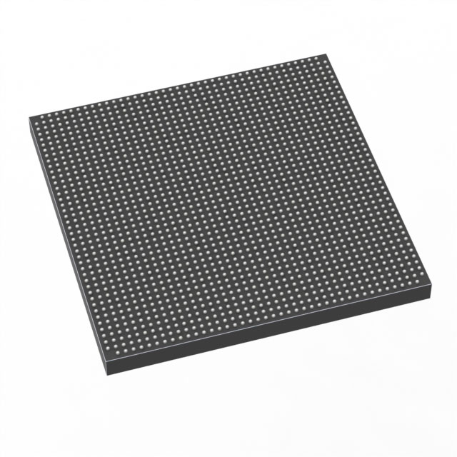
Stratix® 10 GX Field Programmable Gate Array (FPGA) IC 688 850000 1760-BBGA, FCBGA |
|---|---|
| Quantity | 1,875 Available (as of June 15, 2026) |

| Product Category | Field Programmable Gate Array (FPGA) |
|---|---|
| Manufacturer | Intel |
| Manufacturing Status | Active |
| Manufacturer Standard Lead Time | 12 Weeks |
| Datasheet |
Specifications & Environmental
| Device Package | 1760-FBGA (42.5x42.5) | Grade | Industrial | Operating Temperature | -40°C – 100°C | ||
|---|---|---|---|---|---|---|---|
| Package / Case | 1760-BBGA, FCBGA | Number of I/O | 688 | Voltage | 820 mV - 880 mV | ||
| Mounting Method | Surface Mount | RoHS Compliance | Unknown | REACH Compliance | REACH Unaffected | ||
| Moisture Sensitivity Level | 3 (168 Hours) | Number of LABs/CLBs | 106250 | Number of Logic Elements/Cells | 850000 | ||
| Number of Gates | N/A | ECCN | N/A | HTS Code | N/A | ||
| Qualification | N/A | Total RAM Bits | 71303168 |
Overview of 1SG085HN1F43I2LG – Stratix® 10 GX FPGA IC, 850,000 logic elements, 688 I/Os, 1760-BBGA
The 1SG085HN1F43I2LG is an Intel Stratix® 10 GX field-programmable gate array (FPGA) supplied in a 1760-BBGA (FCBGA) package. It delivers a high logic capacity device profile—850,000 logic elements—and is presented for industrial-grade applications with an operating temperature range of −40 °C to 100 °C.
This device is part of the Stratix 10 GX family, which features innovations such as the Intel Hyperflex core architecture and Intel 14 nm tri-gate (FinFET) technology as described in the family overview. The part pairs large on‑chip RAM (71,303,168 bits) with a high I/O count (688) and a low-voltage core supply range (820 mV to 880 mV).
Key Features
- Core & architecture Part of the Intel Stratix 10 GX family, which includes the Intel Hyperflex core architecture and Intel 14 nm tri‑gate (FinFET) technology as highlighted in the device overview.
- Logic capacity Approximately 850,000 logic elements for large, complex FPGA designs.
- On‑chip memory Total RAM of 71,303,168 bits for buffering, packet processing, and on‑chip data storage.
- I/O and packaging 688 general-purpose I/Os in a surface‑mount 1760‑BBGA (1760‑FBGA, 42.5 × 42.5 mm) package to support high pin-count interfaces.
- Power supply Core voltage supply range of 820 mV to 880 mV to support the device’s power domain requirements.
- Temperature & grade Industrial grade with an operating temperature range from −40 °C to 100 °C.
- RoHS compliance RoHS‑compliant manufacturing status.
Typical Applications
- High‑performance networking Large logic capacity and extensive on‑chip RAM enable packet processing, switching, and protocol implementation using the device’s high I/O density.
- Data center acceleration High logic element count and significant RAM support hardware acceleration tasks, in designs requiring dense FPGA fabric and plentiful I/O.
- Telecommunications infrastructure Industrial temperature rating and large I/O count suit telecom gear and infrastructure equipment deployed in controlled or harsh environments.
- Test and measurement High logic density and abundant I/O allow implementation of complex signal processing and multi‑channel capture/analysis systems.
Unique Advantages
- High logic density: 850,000 logic elements provide the headroom to implement large, multi‑function FPGA designs without partitioning across multiple devices.
- Substantial on‑chip memory: 71,303,168 bits of RAM reduce dependence on external memory for intermediate buffering and fast data paths.
- Extensive I/O capability: 688 I/Os in a compact 1760‑BBGA package enable many parallel interfaces and high pin‑count designs in a single device.
- Industrial temperature rating: Specified operation from −40 °C to 100 °C supports deployment in industrial and temperature‑variable environments.
- Low‑voltage core operation: Core supply range of 820 mV–880 mV supports modern low‑voltage power architectures.
- Compliance and manufacturability: Surface‑mount 1760‑FBGA package and RoHS compliance align with standard industrial production and environmental requirements.
Why Choose 1SG085HN1F43I2LG?
The 1SG085HN1F43I2LG positions itself for designs that require high logic capacity, large on‑chip memory, and a high I/O count within an industrial temperature envelope. As a member of the Intel Stratix 10 GX family, the device benefits from the family’s architectural innovations while providing specific, verifiable resources—850,000 logic elements, 71,303,168 bits of RAM, and 688 I/Os—needed for demanding FPGA implementations.
This part is suitable for engineering teams building complex communications, data‑acceleration, or industrial control systems that require dense FPGA fabric and robust thermal performance. Its package, voltage, and compliance characteristics help simplify board‑level integration and production planning.
Request a quote or submit a pricing/availability inquiry to receive technical and commercial details for 1SG085HN1F43I2LG.


Date Founded: 1968
Headquarters: Santa Clara, California, USA
Employees: 130,000+
Revenue: $54.23 Billion
Certifications and Memberships: ISO9001:2015, ISO14001:2015, ISO17025:2017, ISO27001:2022, ISO45001:2018, ISO50001:2018


