
1SG085HN1F43I1VG
| Part Description |
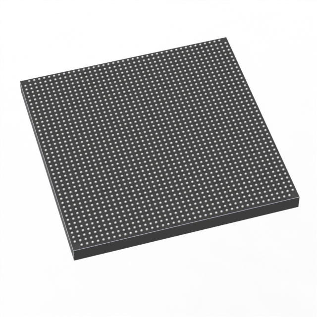
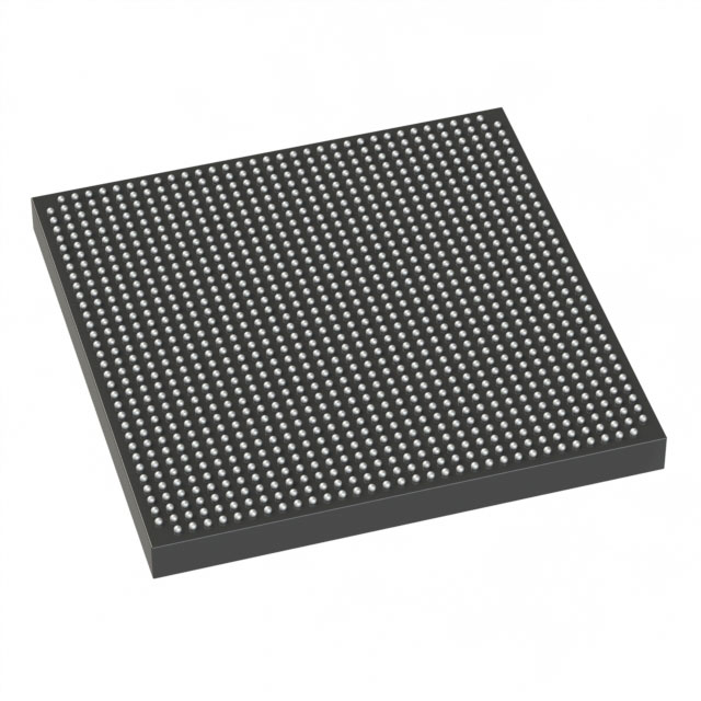
Stratix® 10 GX Field Programmable Gate Array (FPGA) IC 688 850000 1760-BBGA, FCBGA |
|---|---|
| Quantity | 1,872 Available (as of June 10, 2026) |

| Product Category | Field Programmable Gate Array (FPGA) |
|---|---|
| Manufacturer | Intel |
| Manufacturing Status | Active |
| Manufacturer Standard Lead Time | 12 Weeks |
| Datasheet |
Specifications & Environmental
| Device Package | 1760-FBGA (42.5x42.5) | Grade | Industrial | Operating Temperature | -40°C – 100°C | ||
|---|---|---|---|---|---|---|---|
| Package / Case | 1760-BBGA, FCBGA | Number of I/O | 688 | Voltage | 770 mV - 970 mV | ||
| Mounting Method | Surface Mount | RoHS Compliance | Unknown | REACH Compliance | REACH Unaffected | ||
| Moisture Sensitivity Level | 3 (168 Hours) | Number of LABs/CLBs | 106250 | Number of Logic Elements/Cells | 850000 | ||
| Number of Gates | N/A | ECCN | N/A | HTS Code | N/A | ||
| Qualification | N/A | Total RAM Bits | 71303168 |
Overview of 1SG085HN1F43I1VG – Stratix® 10 GX FPGA — 850,000 logic elements, 688 I/O, 1760‑FBGA
The 1SG085HN1F43I1VG is an Intel Stratix® 10 GX Field Programmable Gate Array (FPGA) supplied in a 1760‑FBGA (42.5 × 42.5 mm) surface‑mount package. It combines a large programmable fabric with high I/O density and family innovations such as the Intel Hyperflex core architecture and 14 nm tri‑gate process.
Engineered for advanced, high‑performance applications, this device targets designs that require substantial logic capacity, extensive on‑chip memory, and robust I/O connectivity while operating across an industrial temperature range.
Key Features
- Core & architecture — Intel Hyperflex™ core architecture (family feature) designed to improve core performance compared to previous-generation high-performance FPGAs.
- Logic capacity — 850,000 logic elements to implement large, complex designs and custom accelerators.
- Internal memory — 71,303,168 total RAM bits for large on‑chip buffering, state storage, and memory‑intensive algorithms.
- I/O density — 688 I/O pins to support wide parallel interfaces, multiple high‑speed links, and complex board-level routing.
- Transceiver & IP (family capabilities) — Stratix 10 family documentation highlights heterogeneous 3D SiP transceiver tiles, high‑speed transceiver channels and hard IP options such as PCI Express and Ethernet for system integration.
- Power supply — Core voltage range of 770 mV to 970 mV for compatibility with low‑voltage power architectures.
- Package & mounting — 1760‑FBGA (42.5 × 42.5 mm) surface‑mount package for high‑density board implementations.
- Operating temperature — Industrial grade operation from −40 °C to 100 °C for deployment in temperature‑challenging environments.
- Regulatory status — RoHS compliant.
Typical Applications
- High‑performance networking — Use the device’s large logic capacity and extensive I/O to implement packet processing, switching, and custom network functions.
- Data center acceleration — Implement custom compute kernels and hardware accelerators that leverage the device’s sizable on‑chip memory and logic resources.
- High‑speed communications — Deploy wide parallel interfaces and multiple high‑speed links using the abundant I/O and Stratix 10 family transceiver capabilities.
- Signal processing and DSP — Support complex, memory‑intensive signal processing tasks that require large logic arrays and substantial internal RAM.
Unique Advantages
- Substantial logic resources: 850,000 logic elements provide headroom for complex SoC‑style designs and large FPGA implementations.
- Large on‑chip RAM: Over 71 million bits of internal RAM enable extensive buffering and stateful processing without immediate reliance on external memory.
- High I/O count: 688 I/O pins simplify routing of wide buses and multiple external interfaces, reducing the need for external multiplexing logic.
- Industrial thermal range: Rated for −40 °C to 100 °C operation, supporting deployments in demanding temperature environments.
- Compact, high‑density package: 1760‑FBGA (42.5 × 42.5 mm) package accommodates high pin counts while conserving board area.
- Power‑aware core voltage: Operates in a core voltage window of 770–970 mV to align with low‑voltage power domains.
Why Choose 1SG085HN1F43I1VG?
The 1SG085HN1F43I1VG positions itself as a high‑capacity Stratix® 10 GX FPGA choice for engineers who need substantial programmable logic, generous on‑chip memory, and dense I/O in a single surface‑mount package. Its industrial temperature rating and RoHS compliance make it suitable for demanding embedded and communications applications.
Designed around family innovations such as the Intel Hyperflex core architecture and 14 nm tri‑gate technology, this device offers a platform that scales for complex, high‑performance designs while aligning with modern low‑voltage power domains and high‑density packaging requirements.
Request a quote or submit an RFQ to purchase the 1SG085HN1F43I1VG and discuss availability and lead times.


Date Founded: 1968
Headquarters: Santa Clara, California, USA
Employees: 130,000+
Revenue: $54.23 Billion
Certifications and Memberships: ISO9001:2015, ISO14001:2015, ISO17025:2017, ISO27001:2022, ISO45001:2018, ISO50001:2018


