
1SG280HN1F43E1VGAS
| Part Description |
Stratix® 10 GX Field Programmable Gate Array (FPGA) IC 688 2800000 1760-BBGA, FCBGA |
|---|---|
| Quantity | 1,035 Available (as of June 15, 2026) |

| Product Category | Field Programmable Gate Array (FPGA) |
|---|---|
| Manufacturer | Intel |
| Manufacturing Status | Active |
| Manufacturer Standard Lead Time | 12 Weeks |
| Datasheet |
Specifications & Environmental
| Device Package | 1760-FBGA (42.5x42.5) | Grade | Extended | Operating Temperature | 0°C – 100°C | ||
|---|---|---|---|---|---|---|---|
| Package / Case | 1760-BBGA, FCBGA | Number of I/O | 688 | Voltage | 770 mV - 970 mV | ||
| Mounting Method | Surface Mount | RoHS Compliance | Unknown | REACH Compliance | REACH Unaffected | ||
| Moisture Sensitivity Level | 3 (168 Hours) | Number of LABs/CLBs | 350000 | Number of Logic Elements/Cells | 2800000 | ||
| Number of Gates | N/A | ECCN | N/A | HTS Code | N/A | ||
| Qualification | N/A | Total RAM Bits | 240123904 |
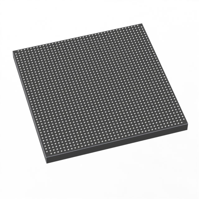
Overview of 1SG280HN1F43E1VGAS – Stratix® 10 GX Field Programmable Gate Array (FPGA), 2,800,000 logic elements, 1760-BBGA
The 1SG280HN1F43E1VGAS is a Stratix® 10 GX family FPGA in a 1760-BBGA (FCBGA) package designed for high-performance, bandwidth‑intensive systems. It pairs a large programmable fabric with extensive on‑chip RAM and high I/O density to address data center, networking, and communications applications that require significant logic resources, embedded memory, and high-speed connectivity.
Built around the Stratix 10 GX device family innovations, this device targets designs that need high core performance and integration—providing a combination of logic capacity, memory, transceiver capability, and low‑voltage core operation for power‑sensitive designs.
Key Features
- Core architecture Stratix 10 GX family innovations and Hyperflex core architecture (family-level) deliver increased core performance for demanding FPGA tasks.
- Logic capacity 2,800,000 logic elements suitable for large-scale digital designs and complex system integration.
- Embedded memory 240,123,904 total RAM bits to support large buffering, on‑chip data stores, and memory‑intensive algorithms.
- I/O and connectivity 688 I/O pins for flexible interfacing to external devices and high‑density system routing.
- Transceiver and high-speed I/O (family-level) Stratix 10 GX family documentation describes heterogeneous 3D SiP transceiver tiles and high-rate transceiver options for high-throughput serial links.
- Package and mounting 1760-BBGA (FCBGA) surface-mount package; supplier package dimension 1760-FBGA (42.5 × 42.5 mm) for compact, board-level integration.
- Power and supply Core voltage range 770 mV to 970 mV to support low-voltage, high-performance operation.
- Operating range and grade Extended grade with an operating temperature range of 0 °C to 100 °C; RoHS‑compliant.
- Family-level system features Stratix 10 GX family-level capabilities include 14 nm tri‑gate (FinFET) technology, hard IP for common interfaces, programmable clocking, and device security/configuration options.
Typical Applications
- Data center and networking — High logic capacity, large embedded RAM, and high I/O density make this FPGA suitable for packet processing, switch/router offload, and network acceleration tasks.
- Telecommunications infrastructure — Family-level high-speed transceivers and large programmable fabric support transport, fronthaul/backhaul, and baseband processing functions.
- High-performance computing and acceleration — Large logic and memory resources enable custom compute kernels, DSP pipelines, and hardware acceleration for compute‑intensive workloads.
- Test, measurement, and instrumentation — High I/O count and substantial on‑chip memory provide the deterministic timing and buffering needed for complex instrumentation systems.
Unique Advantages
- Large programmable capacity: 2.8 million logic elements allow implementation of extensive custom logic and system integration within a single device.
- Significant on‑chip memory: 240,123,904 total RAM bits reduce dependence on external memory for many buffering and data‑path needs.
- High I/O density: 688 I/Os give design flexibility for connecting to multiple peripherals, interfaces, and high-speed PHYs.
- Compact system package: 1760‑FBGA (42.5 × 42.5 mm) package supports high-density board layouts while keeping a large FPGA footprint.
- Low‑voltage core operation: 770 mV–970 mV supply supports modern low-power core domains in complex systems.
- Extended temperature grade: Rated 0 °C to 100 °C for use in a wide range of commercial and enterprise environments.
Why Choose 1SG280HN1F43E1VGAS?
The 1SG280HN1F43E1VGAS provides a balance of high logic density, substantial embedded RAM, and broad I/O capability in a single Stratix 10 GX FPGA package. It is positioned for engineers building systems that demand large programmable fabrics and high data throughput while operating at low core voltage.
This device is suitable for complex networking, communications, and compute acceleration designs that benefit from family-level innovations such as advanced core architecture, high-speed transceiver options, and integrated system features. Its extended temperature grade and RoHS compliance support deployment in controlled commercial and enterprise environments where reliability and long-term availability are important.
Request a quote or contact sales to inquire about availability, pricing, and lead time for the 1SG280HN1F43E1VGAS.


Date Founded: 1968
Headquarters: Santa Clara, California, USA
Employees: 130,000+
Revenue: $54.23 Billion
Certifications and Memberships: ISO9001:2015, ISO14001:2015, ISO17025:2017, ISO27001:2022, ISO45001:2018, ISO50001:2018


