
1SG280HH3F55I3VG
| Part Description |
Stratix® 10 GX Field Programmable Gate Array (FPGA) IC 1160 2800000 2912-BBGA, FCBGA |
|---|---|
| Quantity | 1,050 Available (as of June 10, 2026) |

| Product Category | Field Programmable Gate Array (FPGA) |
|---|---|
| Manufacturer | Intel |
| Manufacturing Status | Active |
| Manufacturer Standard Lead Time | 12 Weeks |
| Datasheet |
Specifications & Environmental
| Device Package | 2912-FBGA, FC (55x55) | Grade | Industrial | Operating Temperature | -40°C – 100°C | ||
|---|---|---|---|---|---|---|---|
| Package / Case | 2912-BBGA, FCBGA | Number of I/O | 1160 | Voltage | 770 mV - 970 mV | ||
| Mounting Method | Surface Mount | RoHS Compliance | Unknown | REACH Compliance | REACH Unaffected | ||
| Moisture Sensitivity Level | 3 (168 Hours) | Number of LABs/CLBs | 350000 | Number of Logic Elements/Cells | 2800000 | ||
| Number of Gates | N/A | ECCN | N/A | HTS Code | N/A | ||
| Qualification | N/A | Total RAM Bits | 240123904 |
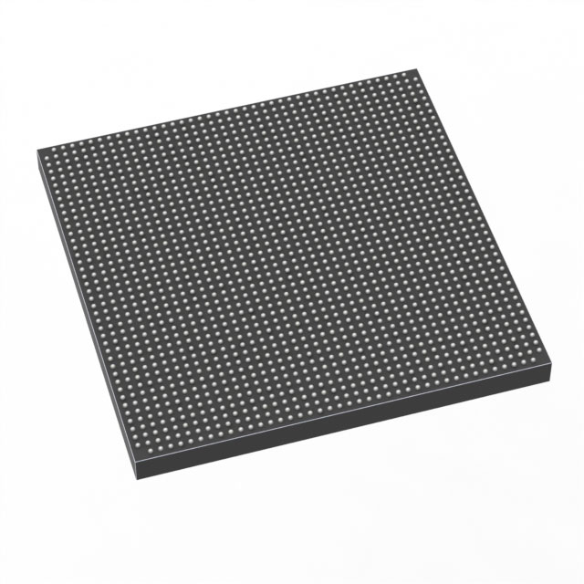
Overview of 1SG280HH3F55I3VG – Stratix® 10 GX FPGA, 2912‑BBGA (FCBGA), 1160 I/O
The 1SG280HH3F55I3VG is an Intel Stratix® 10 GX field programmable gate array (FPGA) device configured in a 2912‑ball FCBGA package. As part of the Stratix 10 GX family, this device leverages the family’s Hyperflex core architecture and Intel 14 nm tri‑gate (FinFET) technology to address high‑performance, high‑bandwidth system requirements.
With 2,800,000 logic elements, extensive on‑chip RAM, and 1,160 user I/Os, this FPGA is targeted at demanding applications that require dense logic, large embedded memory, and wide I/O connectivity while operating across an industrial temperature range.
Key Features
- Core Architecture Part of the Stratix 10 GX family featuring the Intel Hyperflex core architecture and Intel 14 nm tri‑gate (FinFET) process; family devices deliver up to 2× core performance and up to 70% lower power versus the previous generation.
- Logic Density 2,800,000 logic elements for large, complex designs requiring high gate count and implementation flexibility.
- Embedded Memory 240,123,904 total RAM bits of on‑chip memory to support large buffers, tables, and data‑intensive processing.
- I/O and Connectivity 1,160 user I/Os to support broad interface and peripheral requirements; family-level transceiver technology supports high‑speed serial links (family documentation references transceiver data rates and advanced transceiver tiles).
- Power Core supply operating range 770 mV to 970 mV, enabling optimized core voltage selection for power and performance tradeoffs.
- Package and Mounting 2912‑BBGA (55×55) FCBGA package, surface mount, suitable for high‑density board integration.
- Temperature and Grade Industrial grade with an operating temperature range of −40°C to 100°C for deployment in thermally challenging environments.
Typical Applications
- High‑Performance Networking Packet processing, switching, and backplane applications that require dense logic and large on‑chip memory for buffering and packet manipulation.
- Data Center Acceleration Custom compute and I/O acceleration tasks that need high logic capacity and extensive I/O to interface with host systems and memory subsystems.
- High‑Speed Serial Communications Applications leveraging family transceiver capabilities for multi‑lane serial links and high‑bandwidth chip‑to‑chip or backplane connections.
- DSP and Signal Processing Throughput‑intensive signal processing implementations using large embedded RAM and dense logic resources.
Unique Advantages
- High Logic Capacity: 2.8 million logic elements provide the resource headroom required for large FPGA designs and complex IP integration.
- Large On‑Chip Memory: 240,123,904 total RAM bits reduce dependence on external memory for many buffering and stateful processing tasks.
- Extensive I/O Count: 1,160 I/Os enable broad interfacing options for systems with multiple peripherals, external memory, and high‑speed links.
- Industrial Temperature Range: Rated for −40°C to 100°C operation to support industrial and ruggedized system requirements.
- Scalable Stratix 10 Family Architecture: Family innovations such as Hyperflex cores and 14 nm FinFET process provide a clear upgrade path and performance/power advantages compared to previous generation devices.
- Compact, High‑Density Package: 2912‑ball FCBGA (55×55) enables high integration density on compact PCBs.
Why Choose 1SG280HH3F55I3VG?
The 1SG280HH3F55I3VG positions itself as a high‑density, industrial‑grade Stratix 10 GX FPGA option for systems demanding large logic capacity, substantial embedded RAM, and broad I/O. Its family‑level architecture and 14 nm FinFET implementation deliver the performance and efficiency advantages described in the Stratix 10 GX documentation.
This device is well suited to designers building high‑bandwidth networking, data center acceleration, or signal processing equipment that must operate reliably across an industrial temperature range while taking advantage of the Stratix 10 family’s advanced core and transceiver capabilities.
Request a quote or submit an inquiry to receive pricing and availability for the 1SG280HH3F55I3VG and to discuss how it fits your next high‑performance FPGA design.


Date Founded: 1968
Headquarters: Santa Clara, California, USA
Employees: 130,000+
Revenue: $54.23 Billion
Certifications and Memberships: ISO9001:2015, ISO14001:2015, ISO17025:2017, ISO27001:2022, ISO45001:2018, ISO50001:2018


