
1SG280HH3F55E3XG
| Part Description |
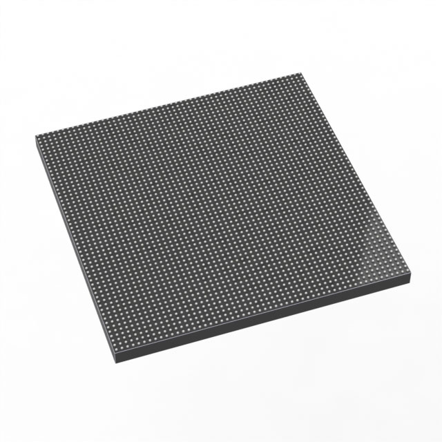
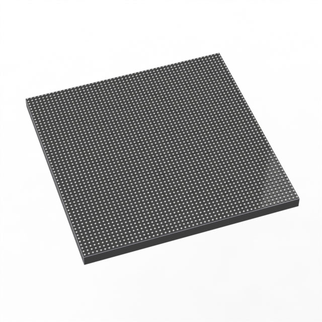
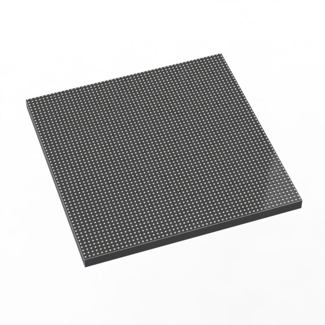
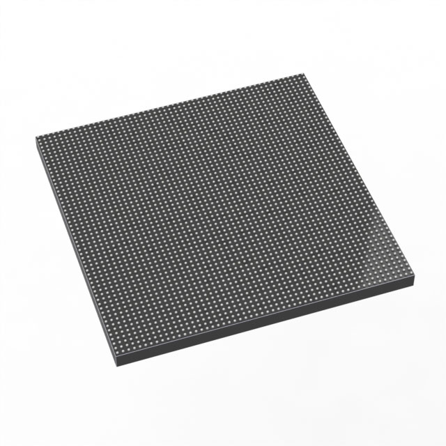
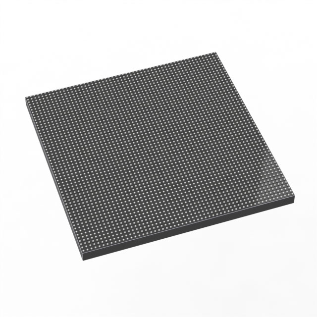
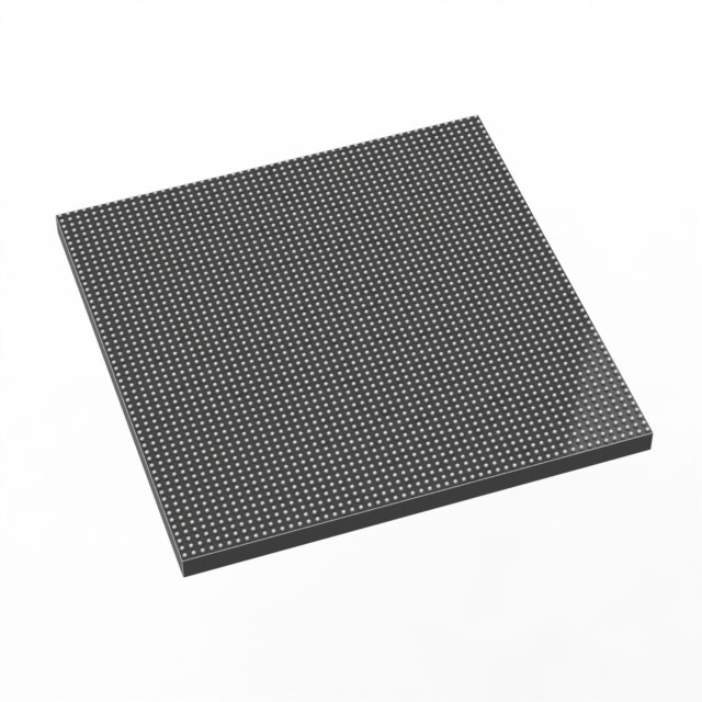
Stratix® 10 GX Field Programmable Gate Array (FPGA) IC 1160 2800000 2912-BBGA, FCBGA |
|---|---|
| Quantity | 274 Available (as of October 8, 2026) |
| Product Category | Field Programmable Gate Array (FPGA) |
|---|---|
| Manufacturer | Intel |
| Manufacturing Status | Active |
| Manufacturer Standard Lead Time | 12 Weeks |
| Datasheet |
Specifications & Environmental
| Device Package | 2912-FBGA, FC (55x55) | Grade | Extended | Operating Temperature | 0°C – 100°C | ||
|---|---|---|---|---|---|---|---|
| Package / Case | 2912-BBGA, FCBGA | Number of I/O | 1160 | Voltage | 820 mV - 880 mV | ||
| Mounting Method | Surface Mount | RoHS Compliance | Unknown | REACH Compliance | REACH Unaffected | ||
| Moisture Sensitivity Level | 3 (168 Hours) | Number of LABs/CLBs | 350000 | Number of Logic Elements/Cells | 2800000 | ||
| Number of Gates | N/A | ECCN | N/A | HTS Code | N/A | ||
| Qualification | N/A | Total RAM Bits | 240123904 |
Overview of 1SG280HH3F55E3XG – Stratix® 10 GX Field Programmable Gate Array (FPGA), 2,800,000 logic elements, 2912-BBGA
The 1SG280HH3F55E3XG is an Intel Stratix® 10 GX FPGA providing high-density programmable logic and extensive on-chip memory for demanding bandwidth- and compute-intensive designs. Built on the Stratix 10 GX family architecture, it leverages the Intel Hyperflex core and advanced process technologies to deliver elevated core performance and energy efficiency for data- and signal-processing systems.
This device targets high-performance communications, networking, and compute applications that require large logic capacity, abundant embedded RAM, and extensive I/O. Key value comes from its combination of 2,800,000 logic elements, 240,123,904 total RAM bits, and 1,160 I/O pins in a 2912-BBGA package.
Key Features
- Core & Architecture Intel Hyperflex core architecture and Stratix 10 family innovations deliver increased core performance and improved power efficiency as documented for the family.
- Logic Capacity 2,800,000 logic elements provide a very high level of programmable logic resources for complex logic, packet processing, and custom compute pipelines.
- On‑Chip Memory 240,123,904 total RAM bits of embedded memory support large buffering, lookup tables, and memory-intensive algorithms without immediate reliance on external DRAM.
- I/O & Transceiver Capability 1,160 I/O pins enable extensive board-level interfacing options. Family-level transceiver and high-speed I/O innovations are part of the Stratix 10 GX device overview.
- Voltage & Power Core voltage supply range of 820 mV to 880 mV enables operation within the specified low-voltage core domain for this device.
- Package & Mounting Supplied in a 2912-BBGA (FCBGA) package (2912-FBGA, FC 55×55 footprint) suitable for surface-mount assembly on high-density boards.
- Operating Range & Grade Extended-grade device with an operating temperature range of 0 °C to 100 °C to match thermally constrained system environments.
- Standards & Compliance RoHS compliant to support regulatory and environmental requirements for lead-free assemblies.
Typical Applications
- High‑Performance Networking Packet processing and switching fabrics benefiting from large logic capacity and abundant on-chip RAM for buffering and stateful operations.
- Data Center & Acceleration Compute acceleration, protocol offload, and custom data-path processing where high logic density and extensive I/O are required.
- High‑Speed Communications Backplane, optical, and module-level interfaces that take advantage of the Stratix 10 GX family’s high-speed I/O and transceiver capabilities.
- Signal Processing & DSP Wideband signal chains and real-time processing pipelines that need large embedded memory and dense logic resources.
Unique Advantages
- High Logic Density: 2,800,000 logic elements enable consolidation of complex functions into a single device, reducing board-level component count.
- Large Embedded Memory: 240,123,904 RAM bits provide significant on-chip storage for packet buffers, lookup tables, and streaming data without immediate external memory dependencies.
- Extensive I/O Count: 1,160 I/O pins support rich peripheral and protocol interfacing options, simplifying multi-lane and multi-protocol designs.
- Advanced Core Efficiency: Family-level Hyperflex core architecture improvements help deliver higher core performance and improved power characteristics versus earlier generations.
- Compact Surface‑Mount Package: 2912-BBGA FCBGA packaging in a 55×55 footprint balances routeability and thermal considerations for dense system boards.
- RoHS Compliance & Extended Grade: Environmentally compliant materials and extended-grade temperature range support a wide array of commercial and enterprise applications.
Why Choose 1SG280HH3F55E3XG?
The 1SG280HH3F55E3XG positions itself as a high-density, high-performance Stratix 10 GX FPGA option for designs demanding substantial programmable logic, large on-chip RAM, and broad I/O. Its combination of family-level architectural innovations and device-level capacity makes it well suited for networking, data-center acceleration, high-speed communications, and advanced signal-processing systems.
Designed for engineers and system architects who need scalable logic resources and integrated memory in a single-package FPGA, this device offers long-term design flexibility through high density, proven family features, and compliance with RoHS environmental standards.
Request a quote or submit a purchase inquiry to learn pricing, availability, and how the 1SG280HH3F55E3XG can meet your project requirements.





















Date Founded: 1968
Headquarters: Santa Clara, California, USA
Employees: 130,000+
Revenue: $54.23 Billion
Certifications and Memberships: ISO9001:2015, ISO14001:2015, ISO17025:2017, ISO27001:2022, ISO45001:2018, ISO50001:2018


