
1ST040EH3F35E3XG
| Part Description |
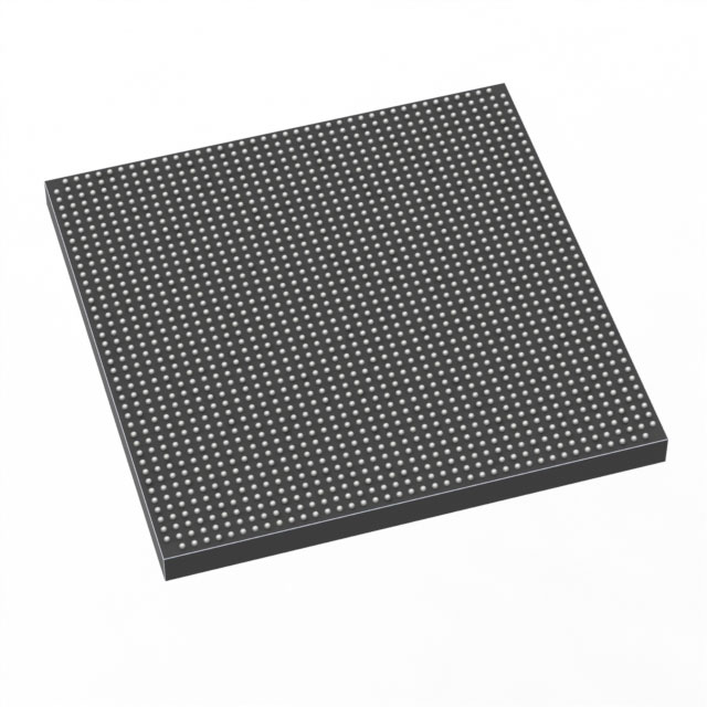
Stratix® 10 TX Field Programmable Gate Array (FPGA) IC 384 31457280 378000 1152-BBGA, FCBGA |
|---|---|
| Quantity | 810 Available (as of June 18, 2026) |

| Product Category | Field Programmable Gate Array (FPGA) |
|---|---|
| Manufacturer | Intel |
| Manufacturing Status | Active |
| Manufacturer Standard Lead Time | 12 Weeks |
| Datasheet |
Specifications & Environmental
| Device Package | 1152-FBGA (35x35) | Grade | Extended | Operating Temperature | 0°C – 100°C | ||
|---|---|---|---|---|---|---|---|
| Package / Case | 1152-BBGA, FCBGA | Number of I/O | 384 | Voltage | 870 mV - 970 mV | ||
| Mounting Method | Surface Mount | RoHS Compliance | Unknown | REACH Compliance | REACH Unknown | ||
| Moisture Sensitivity Level | 3 (168 Hours) | Number of LABs/CLBs | N/A | Number of Logic Elements/Cells | 378000 | ||
| Number of Gates | N/A | ECCN | N/A | HTS Code | N/A | ||
| Qualification | N/A | Total RAM Bits | 31457280 |
Overview of 1ST040EH3F35E3XG – Stratix® 10 TX Field Programmable Gate Array (FPGA) IC
The 1ST040EH3F35E3XG is a Stratix® 10 TX field programmable gate array (FPGA) IC from Intel, supplied in a 1152-FBGA (35×35) package. It provides a high-density programmable logic fabric with substantial on-chip memory and I/O to support demanding digital designs.
With 378,000 logic elements, 31,457,280 total RAM bits and 384 I/O pins, this device is aimed at applications that require large logic capacity, significant embedded memory, and extensive board-level connectivity while operating within a low-voltage supply range and an extended temperature window.
Key Features
- Core Logic Capacity — 378,000 logic elements for implementing large-scale custom digital designs and complex logic networks.
- On-Chip Memory — 31,457,280 total RAM bits to support data buffering, caching and state storage close to the logic fabric.
- I/O Count — 384 I/O pins to enable broad external connectivity and interface options on the system board.
- Power Supply — Operates from 870 mV to 970 mV, enabling compatibility with low-voltage power domains.
- Package — 1152-BBGA, FCBGA (1152-FBGA, 35×35) surface-mount package for compact board integration.
- Temperature & Grade — Extended grade with an operating temperature range of 0 °C to 100 °C for applications requiring extended-range operation.
- RoHS Compliance — Device is RoHS compliant.
Typical Applications
- High-density logic implementations — Use the 378,000 logic elements to consolidate complex digital functions and custom logic into a single FPGA.
- Memory-intensive designs — Leverage 31,457,280 RAM bits for on-chip buffering, large FIFOs or local data storage close to processing logic.
- I/O-rich systems — 384 I/Os support designs that require multiple external interfaces or parallel signal paths.
- Compact board-level integration — The 1152-FBGA (35×35) surface-mount package enables high-density placement in space-constrained systems.
Unique Advantages
- Substantial programmable capacity: A large count of logic elements lets designers implement complex algorithms and consolidate functions that might otherwise require multiple devices.
- Significant embedded memory: Tens of millions of RAM bits reduce external memory dependence and improve data locality for latency-sensitive tasks.
- Extensive I/O availability: 384 I/Os simplify the implementation of multiple interfaces and parallel connections without heavy I/O multiplexing.
- Low-voltage operation: The 870 mV to 970 mV supply range supports integration into modern low-voltage power domains.
- Compact, standardized package: The 1152-FBGA (35×35) surface-mount package supports dense board layouts and consistent assembly processes.
- Extended operating range: Grade and 0 °C to 100 °C operating window accommodate designs requiring extended-temperature operation.
Why Choose 1ST040EH3F35E3XG?
The 1ST040EH3F35E3XG positions itself as a high-capacity Stratix® 10 TX FPGA option combining large programmable logic resources, extensive on-chip memory, and broad I/O in a compact FBGA package. These characteristics make it suitable for system designs where consolidation of logic, substantial local memory, and numerous external interfaces are priorities.
Designed and manufactured by Intel, this device offers a balance of scalability and integration for engineering teams developing complex digital systems that must operate within a low-voltage domain and an extended temperature range. It suits customers looking for a single-device solution to reduce BOM complexity and maintain headroom for future design iterations.
Request a quote or submit an inquiry to receive pricing and availability information for the 1ST040EH3F35E3XG. Our team can assist with lead times and volume options tailored to your project needs.


Date Founded: 1968
Headquarters: Santa Clara, California, USA
Employees: 130,000+
Revenue: $54.23 Billion
Certifications and Memberships: ISO9001:2015, ISO14001:2015, ISO17025:2017, ISO27001:2022, ISO45001:2018, ISO50001:2018


