
1ST250EY1F55I1VG
| Part Description |
Stratix® 10 TX Field Programmable Gate Array (FPGA) IC 296 2500000 2912-BBGA, FCBGA |
|---|---|
| Quantity | 1,297 Available (as of June 15, 2026) |

| Product Category | Field Programmable Gate Array (FPGA) |
|---|---|
| Manufacturer | Intel |
| Manufacturing Status | Active |
| Manufacturer Standard Lead Time | 12 Weeks |
| Datasheet |
Specifications & Environmental
| Device Package | 2912-FBGA, FC (55x55) | Grade | Industrial | Operating Temperature | -40°C – 100°C | ||
|---|---|---|---|---|---|---|---|
| Package / Case | 2912-BBGA, FCBGA | Number of I/O | 296 | Voltage | 770 mV - 970 mV | ||
| Mounting Method | Surface Mount | RoHS Compliance | Unknown | REACH Compliance | REACH Unaffected | ||
| Moisture Sensitivity Level | 3 (168 Hours) | Number of LABs/CLBs | 312500 | Number of Logic Elements/Cells | 2500000 | ||
| Number of Gates | N/A | ECCN | N/A | HTS Code | N/A | ||
| Qualification | N/A | Total RAM Bits | 204472320 |
Overview of 1ST250EY1F55I1VG – Stratix® 10 TX FPGA, 2,500,000 logic elements, 296 I/O, 2912-BBGA
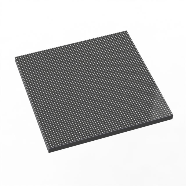
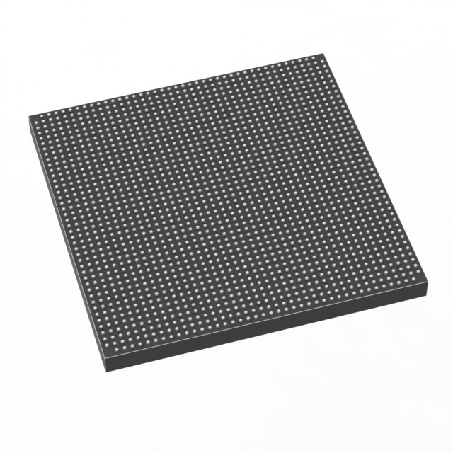
The 1ST250EY1F55I1VG is an Intel Stratix® 10 TX Field Programmable Gate Array provided in a 2912-ball flip‑chip BGA (55 × 55 mm) package. This industrial-grade device integrates a large monolithic FPGA fabric with high-density I/O and substantial on-chip RAM to address demanding, bandwidth‑intensive system designs.
As part of the Stratix 10 TX family, the device benefits from the family’s HyperFlex® core architecture and high‑speed transceiver innovations, making it suitable for applications that require massive logic capacity, extensive internal memory, and high-speed serial connectivity.
Key Features
- Logic Capacity Provides 2,500,000 logic elements for implementation of large, complex digital designs and high-density custom logic.
- On‑chip Memory Includes 204,472,320 total RAM bits to support large data buffers, packet processing, and stateful algorithms without constant external memory access.
- I/O and Packaging Offers 296 I/O pins in a 2912‑BBGA FCBGA package (supplier package: 2912‑FBGA, FC 55×55), supporting dense board routing and robust signal routing in compact footprints.
- High‑speed Transceiver Architecture (Family Feature) Stratix 10 TX family devices include dual‑mode transceivers capable of 57.8 Gbps PAM4 and 28.9 Gbps NRZ operation for chip‑to‑chip, chip‑to‑module, and backplane links.
- Core Architecture (Family Feature) HyperFlex® core architecture is documented to deliver increased core performance compared to previous generation high‑performance FPGAs.
- Hard IP (Family Feature) Family documentation lists hardened PCIe Gen3 and multi‑rate Ethernet MAC IP blocks useful for accelerating common system interfaces.
- Supply Voltage Range Operates from 770 mV to 970 mV for core voltage domains, enabling integration with modern low‑voltage power supplies.
- Industrial Temperature Grade Specified for operation from −40 °C to 100 °C, suitable for industrial environments.
- Environmental Compliance RoHS‑compliant.
Typical Applications
- High‑speed Networking and Telemetry Leverages the Stratix 10 TX family transceiver capability and large logic/memory resources to implement packet processing, aggregation, and line‑rate protocol offload.
- Backplane and Chip‑to‑Module Connectivity Supports high‑bandwidth backplane and board‑to‑board links using dual‑mode transceivers and abundant logic for protocol handling and data steering.
- Compute Acceleration and Data Processing Large logic element count and substantial on‑chip RAM enable custom accelerators, streaming data pipelines, and real‑time signal processing.
- Telecommunications Infrastructure Fits applications requiring hardened interfaces (PCIe, Ethernet MACs) and scalable bandwidth for line cards and network appliances.
Unique Advantages
- Massive Logic Capacity: 2,500,000 logic elements enable integration of complex systems-on‑chip into a single FPGA, reducing external component count.
- Large On‑Chip Memory: Over 204 million bits of RAM reduce reliance on external memory for buffering and stateful processing, improving throughput and latency.
- High‑Speed Serial I/O (Family Advantage): Dual‑mode transceiver support up to 57.8 Gbps PAM4/28.9 Gbps NRZ provides flexible connectivity options for next‑generation links.
- Industrial Thermal Range: Rated from −40 °C to 100 °C to support deployments in industrial environments with wider temperature swings.
- Compact High‑Ball‑Count Package: 2912‑BBGA (55 × 55 mm) delivers high pin density for complex I/O and board‑level integration while conserving PCB area.
- Documented Family‑Level Hard IP: Stratix 10 TX family documentation highlights hardened PCIe and Ethernet MAC IP blocks, reducing design time for standard interfaces.
Why Choose 1ST250EY1F55I1VG?
The 1ST250EY1F55I1VG delivers a combination of very large logic capacity, extensive on‑chip RAM, and a high‑density BGA package tailored for high‑bandwidth, compute‑intensive systems. Its industrial operating range and RoHS compliance make it appropriate for demanding environments where reliability and long‑term availability matter.
Choose this device when your design requires integrating large custom logic functions, substantial internal buffering, and multi‑gigabit serial connectivity while maintaining a compact board footprint. The Stratix 10 TX family features documented performance and hardened IP blocks that help accelerate development for networking, telecom, and high‑performance data processing applications.
If you would like pricing, availability, or a formal quote for 1ST250EY1F55I1VG, submit a request for a quote or contact sales to discuss your requirements and lead‑time.


Date Founded: 1968
Headquarters: Santa Clara, California, USA
Employees: 130,000+
Revenue: $54.23 Billion
Certifications and Memberships: ISO9001:2015, ISO14001:2015, ISO17025:2017, ISO27001:2022, ISO45001:2018, ISO50001:2018


