
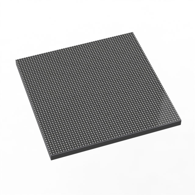
1ST250EY2F55E2LG
| Part Description |
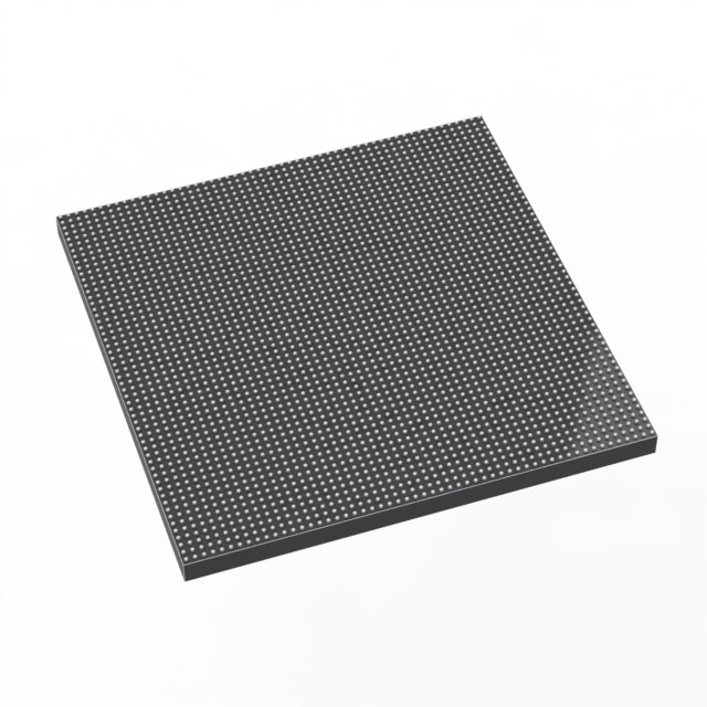
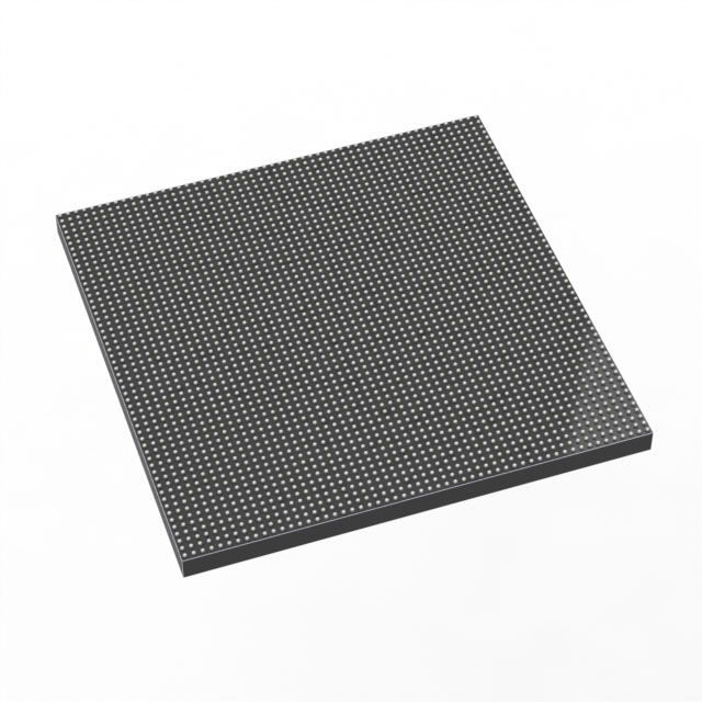
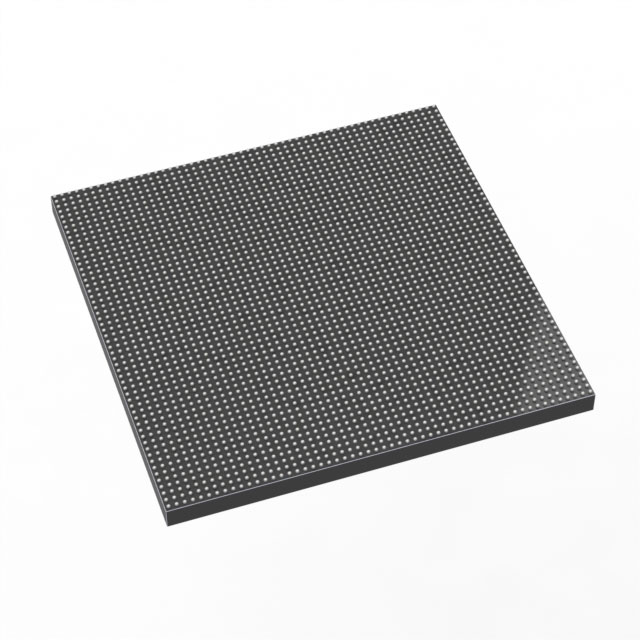
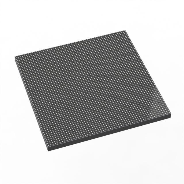
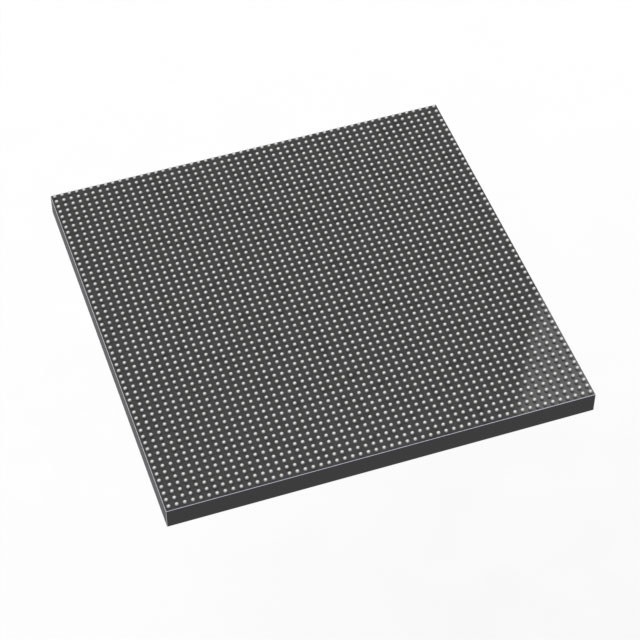
Stratix® 10 TX Field Programmable Gate Array (FPGA) IC 296 2500000 2912-BBGA, FCBGA |
|---|---|
| Quantity | 1,179 Available (as of October 7, 2026) |
| Product Category | Field Programmable Gate Array (FPGA) |
|---|---|
| Manufacturer | Intel |
| Manufacturing Status | Active |
| Manufacturer Standard Lead Time | 12 Weeks |
| Datasheet |
Specifications & Environmental
| Device Package | 2912-FBGA, FC (55x55) | Grade | Extended | Operating Temperature | 0°C – 100°C | ||
|---|---|---|---|---|---|---|---|
| Package / Case | 2912-BBGA, FCBGA | Number of I/O | 296 | Voltage | 820 mV - 880 mV | ||
| Mounting Method | Surface Mount | RoHS Compliance | Unknown | REACH Compliance | REACH Unaffected | ||
| Moisture Sensitivity Level | 3 (168 Hours) | Number of LABs/CLBs | 312500 | Number of Logic Elements/Cells | 2500000 | ||
| Number of Gates | N/A | ECCN | N/A | HTS Code | N/A | ||
| Qualification | N/A | Total RAM Bits | 204472320 |
Overview of 1ST250EY2F55E2LG – Stratix® 10 TX FPGA, 2,500,000 Logic Elements, 2912‑BBGA
The 1ST250EY2F55E2LG is a Stratix® 10 TX field programmable gate array (FPGA) in a 2912‑ball FCBGA package designed for high‑bandwidth, compute‑intensive system designs. It pairs Intel’s HyperFlex core architecture and 14 nm FinFET FPGA fabric with high‑speed transceiver tiles and hardened IP to address demanding communications, data‑center, and networking applications.
This device provides 2,500,000 logic elements, large on‑chip RAM, a broad I/O set, and an extended‑grade operating range, delivering a highly integrated programmable foundation for systems that require high logic density and high aggregate bandwidth.
Key Features
- Core architecture Built on Intel’s HyperFlex™ core architecture and 14 nm tri‑gate (FinFET) process as described for Stratix 10 TX devices, providing a modern high‑performance FPGA fabric.
- Logic density 2,500,000 logic elements (cells) to implement complex digital designs and large custom logic functions.
- On‑chip memory Total RAM of 204,472,320 bits for embedded data storage, buffering, and state retention within the FPGA fabric.
- High‑speed transceivers Stratix 10 TX family dual‑mode transceivers support PAM4 up to 57.8 Gbps and NRZ up to 28.9 Gbps, with support in the family for multi‑channel transceiver tiles and up to 144 full‑duplex channels (family feature).
- Hardened interfaces Family‑level features include hardened PCI Express Gen3 and 10/25/100 Gbps Ethernet MAC IP blocks and Reed‑Solomon FEC support (per Stratix 10 TX device overview).
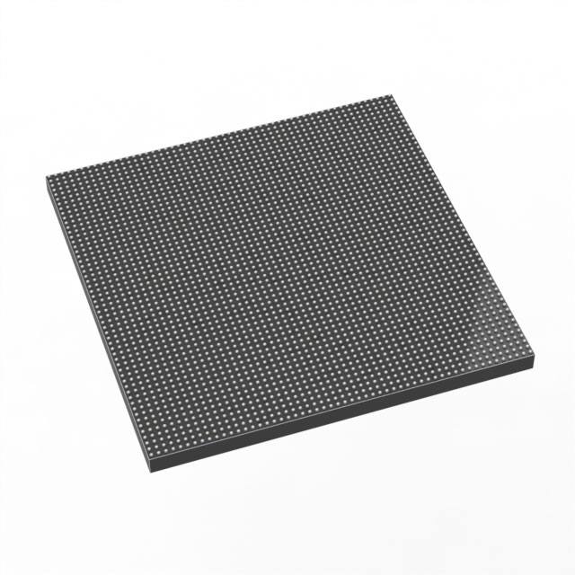
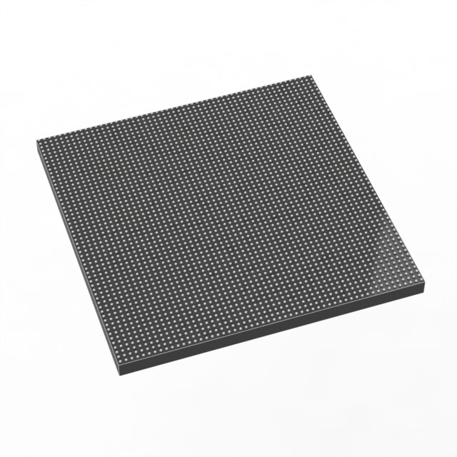
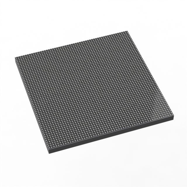
- Package and I/O 2912‑BBGA (FCBGA) supplier device package, 55×55 mm footprint; 296 user I/O pins suitable for dense system interconnects. Surface‑mount package type.
- Power and operating range Core voltage supply range 820 mV to 880 mV; operating temperature range 0 °C to 100 °C; device grade: Extended.
- Compliance RoHS compliant, supporting environmental compliance requirements.
Typical Applications
- High‑speed networking and switching Leverage the Stratix 10 TX transceiver capabilities and hardened Ethernet MAC/FEC blocks for high aggregate bandwidth switching and network line cards.
- Data center acceleration Use the high logic density and large on‑chip RAM for packet processing, traffic management, and custom acceleration tasks where throughput and integration matter.
- Telecommunications backplane and module interfaces Support chip‑to‑chip, chip‑to‑module, and backplane links using dual‑mode transceivers at PAM4 and NRZ data rates.
- High‑performance compute and I/O aggregation Implement complex glue logic, protocol bridging, and high‑speed I/O aggregation with ample logic elements and 296 I/Os.
Unique Advantages
- High logic capacity: 2,500,000 logic elements enable implementation of large, complex digital systems without external discrete logic.
- Substantial on‑chip memory: 204,472,320 bits of RAM reduce dependence on external memory for buffering and accelerate on‑chip data paths.
- Advanced transceiver capability: Family support for dual‑mode 57.8 Gbps PAM4 and 28.9 Gbps NRZ transceivers and multi‑channel transceiver tiles supports high‑bandwidth I/O and flexible link topologies.
- Hardened communication IP: Availability of hardened PCIe Gen3 and high‑speed Ethernet MAC/FEC in the Stratix 10 TX family simplifies integration of standard protocols and reduces custom logic development.
- Compact, production‑ready package: 2912‑BBGA (55×55 mm) surface‑mount package with 296 I/Os provides a dense, manufacturable footprint for system boards.
- Compliance and extended grade: RoHS compliance and an extended operating temperature range (0 °C to 100 °C) support deployment in a wide range of commercial and telecom environments.
Why Choose 1ST250EY2F55E2LG?
The 1ST250EY2F55E2LG combines high logic density, large on‑chip RAM, and Stratix 10 TX family transceiver and hardened IP capabilities in a production‑grade FCBGA package. It is positioned for designers who need a highly integrated, programmable platform for high‑bandwidth communications, data‑center acceleration, and advanced networking equipment.
With a defined voltage supply window and extended operating temperature range, this FPGA provides measurable system design parameters for power and thermal planning while delivering the fabric resources and I/O needed for scalable, long‑lifecycle designs backed by the Stratix 10 TX device family documentation.
Request a quote or submit an inquiry to obtain pricing and availability for the 1ST250EY2F55E2LG and to discuss how it can fit into your next high‑performance FPGA design.





















Date Founded: 1968
Headquarters: Santa Clara, California, USA
Employees: 130,000+
Revenue: $54.23 Billion
Certifications and Memberships: ISO9001:2015, ISO14001:2015, ISO17025:2017, ISO27001:2022, ISO45001:2018, ISO50001:2018


