
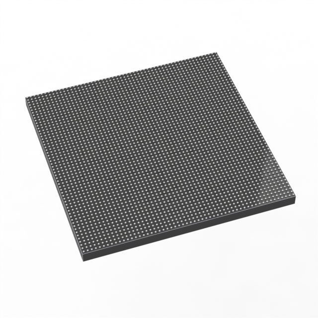
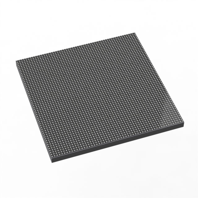
1ST250EY2F55I2VG
| Part Description |
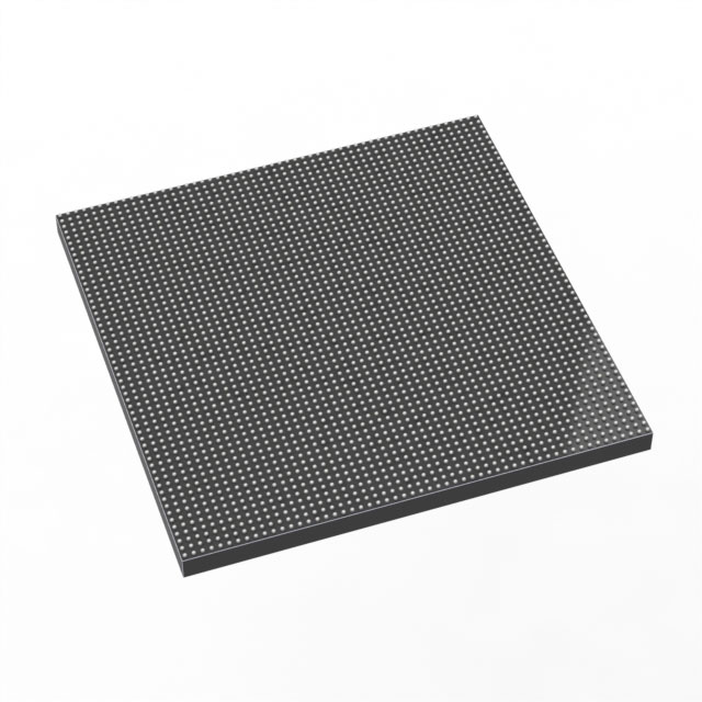
Stratix® 10 TX Field Programmable Gate Array (FPGA) IC 296 2500000 2912-BBGA, FCBGA |
|---|---|
| Quantity | 444 Available (as of October 8, 2026) |
| Product Category | Field Programmable Gate Array (FPGA) |
|---|---|
| Manufacturer | Intel |
| Manufacturing Status | Active |
| Manufacturer Standard Lead Time | 12 Weeks |
| Datasheet |
Specifications & Environmental
| Device Package | 2912-FBGA, FC (55x55) | Grade | Industrial | Operating Temperature | -40°C – 100°C | ||
|---|---|---|---|---|---|---|---|
| Package / Case | 2912-BBGA, FCBGA | Number of I/O | 296 | Voltage | 770 mV - 970 mV | ||
| Mounting Method | Surface Mount | RoHS Compliance | Unknown | REACH Compliance | REACH Unaffected | ||
| Moisture Sensitivity Level | 3 (168 Hours) | Number of LABs/CLBs | 312500 | Number of Logic Elements/Cells | 2500000 | ||
| Number of Gates | N/A | ECCN | N/A | HTS Code | N/A | ||
| Qualification | N/A | Total RAM Bits | 204472320 |
Overview of 1ST250EY2F55I2VG – Stratix® 10 TX FPGA, 2,500,000 logic elements, 2912‑BBGA
The 1ST250EY2F55I2VG is an Intel Stratix® 10 TX Field Programmable Gate Array (FPGA) in a 2912‑BBGA FCBGA package designed for industrial-grade, high-performance designs. It combines a high-density fabric with Intel HyperFlex® core architecture and family-level support for dual-mode high-speed transceivers, delivering a platform optimized for bandwidth‑intensive communications, compute acceleration, and advanced networking applications.
With 2,500,000 logic elements, more than 204 million bits of on-chip RAM, and 296 I/Os, this device targets systems that require large programmable logic capacity, substantial on-chip memory, and high I/O and transceiver bandwidth within a surface-mount BGA package.
Key Features
- High-density logic — 2,500,000 logic elements provide large programmable fabric capacity for complex logic and algorithm implementations.
- Intel HyperFlex® core architecture — Family documentation highlights the HyperFlex architecture designed to increase core performance compared to previous generations.
- Dual‑mode high-speed transceivers — Family-level transceiver capability supports both 57.8 Gbps PAM4 and 28.9 Gbps NRZ operation for chip-to-chip, chip-to-module, and backplane applications.
- Large on-chip memory — 204,472,320 total RAM bits available for buffering, packet processing, and algorithm storage.
- Rich I/O and package — 296 I/Os in a 2912‑BBGA (FCBGA) package; supplier package specified as 2912‑FBGA, FC (55×55). Surface-mount mounting type.
- Industrial temperature range — Rated for operation from −40 °C to 100 °C to meet demanding environmental requirements.
- Low-voltage core supply — Core voltage specified between 770 mV and 970 mV.
- Compliance and manufacturability — RoHS compliant and available in a high‑pin‑count BGA suitable for production assembly.
- Family-level hardened IP — Documentation for the Stratix 10 TX family references hardened PCIe Gen3 and 10/25/100 Gbps Ethernet MAC IP blocks and other hardened functions (family-level capability).
Typical Applications
- Data center networking — High logic density, large on-chip RAM, and high-speed dual‑mode transceivers enable packet processing, switching, and aggregation functions for top-of-rack and spine designs.
- Telecom and transport equipment — Support for PAM4 and NRZ transceiver modes and family-level Ethernet/PCIe hard IP make the device suitable for line cards, fronthaul/backhaul, and transport systems.
- High-performance compute acceleration — Large FPGA fabric and memory complement hardware acceleration of compute kernels, packet inspection, and real‑time processing tasks.
- Chip‑to‑chip and module interfaces — Dual-mode transceivers and high I/O count support high-bandwidth chip-to-chip and chip-to-module interconnects in advanced systems.
Unique Advantages
- Substantial programmable capacity: 2,500,000 logic elements let designers map large, complex designs without immediate partitioning across devices.
- High aggregate bandwidth potential: Family transceiver capabilities (PAM4 and NRZ) and hardened networking IP enable deployment in bandwidth‑intensive systems.
- Significant on‑chip RAM: 204,472,320 bits of RAM reduce external memory dependence for many buffering and processing tasks.
- Industrial readiness: −40 °C to 100 °C operating range and RoHS compliance address demanding environmental and regulatory requirements.
- Compact, production-ready package: 2912‑BBGA (55×55) surface-mount package supports high-pin-count routing in space-constrained board designs.
- Optimized power domain: Core supply specified at 770–970 mV supports designs targeting modern low-voltage FPGA power architectures.
Why Choose 1ST250EY2F55I2VG?
The 1ST250EY2F55I2VG combines a very large logic element count with extensive on-chip memory and high I/O density in an industrial‑grade Stratix 10 TX device. It is positioned for systems that need high programmable capacity, advanced transceiver flexibility, and robust thermal performance in a single, surface‑mount BGA package.
This device is suitable for engineering teams building high-bandwidth networking, telecom infrastructure, and compute‑acceleration solutions that require scalable FPGA resources, significant on-chip memory, and family-level hardened IP capabilities. Its combination of logic density, memory, I/O count, and industrial operating range supports long-term deployment and integration into complex systems.
Request a quote or submit an inquiry to receive pricing, availability, and support information for 1ST250EY2F55I2VG.






















Date Founded: 1968
Headquarters: Santa Clara, California, USA
Employees: 130,000+
Revenue: $54.23 Billion
Certifications and Memberships: ISO9001:2015, ISO14001:2015, ISO17025:2017, ISO27001:2022, ISO45001:2018, ISO50001:2018


