
1ST250EY3F55E3XG
| Part Description |
Stratix® 10 TX Field Programmable Gate Array (FPGA) IC 296 2500000 2912-BBGA, FCBGA |
|---|---|
| Quantity | 1,183 Available (as of June 14, 2026) |

| Product Category | Field Programmable Gate Array (FPGA) |
|---|---|
| Manufacturer | Intel |
| Manufacturing Status | Active |
| Manufacturer Standard Lead Time | 12 Weeks |
| Datasheet |
Specifications & Environmental
| Device Package | 2912-FBGA, FC (55x55) | Grade | Extended | Operating Temperature | 0°C – 100°C | ||
|---|---|---|---|---|---|---|---|
| Package / Case | 2912-BBGA, FCBGA | Number of I/O | 296 | Voltage | 820 mV - 880 mV | ||
| Mounting Method | Surface Mount | RoHS Compliance | Unknown | REACH Compliance | REACH Unaffected | ||
| Moisture Sensitivity Level | 3 (168 Hours) | Number of LABs/CLBs | 312500 | Number of Logic Elements/Cells | 2500000 | ||
| Number of Gates | N/A | ECCN | N/A | HTS Code | N/A | ||
| Qualification | N/A | Total RAM Bits | 204472320 |
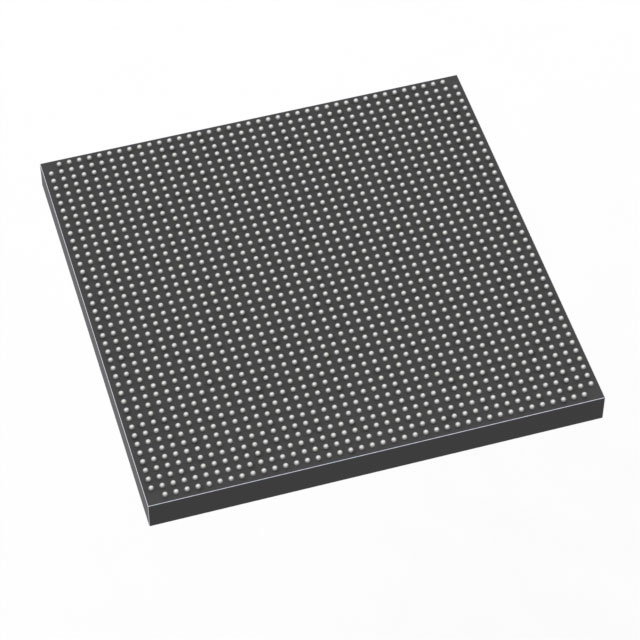
Overview of 1ST250EY3F55E3XG – Stratix® 10 TX FPGA, 2,500,000 logic elements, 2912‑BBGA
The 1ST250EY3F55E3XG is an Intel Stratix® 10 TX field programmable gate array (FPGA) offered in a 2912‑BBGA FCBGA package. It combines a high‑density programmable fabric—2,500,000 logic elements—with large on‑chip RAM to address bandwidth‑intensive and compute‑dense system designs.
Built around the Stratix 10 TX family architecture, this device targets applications that require high transceiver bandwidth, advanced signal processing and system integration, while providing electrical and thermal characteristics suitable for extended‑grade deployments.
Key Features
- High‑density logic — 2,500,000 logic elements (cells) to implement complex programmable logic and large hardware accelerators.
- On‑chip memory — 204,472,320 total RAM bits for buffering, packet processing and deep data paths without immediate dependence on external memory.
- High‑speed transceiver architecture — Series features include dual‑mode transceivers capable of 57.8 Gbps PAM4 and 28.9 Gbps NRZ operation, supporting chip‑to‑chip, chip‑to‑module and backplane link topologies.
- Hard IP for common interfaces — Series documentation describes hardened PCI Express Gen3 and 10/25/100 Gbps Ethernet MAC IP blocks useful for high‑bandwidth interface integration.
- Advanced core architecture — Intel HyperFlex® core architecture (series feature) that improves core performance compared to prior generations.
- DSP and compute blocks — Series includes variable‑precision DSP blocks for signal processing and compute acceleration workloads.
- Package and I/O — 2912‑BBGA (FCBGA) package with 296 I/O pins, supplied in a 2912‑FBGA, FC (55×55) supplier device package format; surface‑mount mounting.
- Power and thermal — Core voltage supply range specified at 820 mV to 880 mV; operating temperature range 0 °C to 100 °C (Extended grade).
- RoHS compliant — Device conforms to RoHS environmental requirements.
Typical Applications
- High‑speed networking and switching — Implements packet processing, forwarding engines and MAC/PHY interfaces leveraging on‑chip memory and hardened Ethernet IP.
- Data center acceleration — Supports hardware acceleration and custom offload functions that require large logic capacity and high aggregate bandwidth.
- Telecommunications and backplane systems — Dual‑mode transceivers and high I/O count enable chip‑to‑module and backplane links for telecom line cards and optical transport equipment.
- Signal processing and compute appliances — Variable‑precision DSP resources and abundant RAM make the device suitable for digital signal processing, encoding/decoding and custom compute pipelines.
Unique Advantages
- Large programmable fabric: 2,500,000 logic elements provide the capacity to consolidate functions that would otherwise require multiple FPGAs, simplifying board design.
- Substantial on‑chip RAM: Over 204 million RAM bits enable deep buffering and local data storage to reduce latency and external memory bandwidth pressure.
- High‑speed serial I/O capability: Dual‑mode transceiver technology described for the Stratix 10 TX family supports modern PAM4 or NRZ links, allowing designers to choose link modes for system requirements.
- Extended‑grade operation: Rated for 0 °C to 100 °C operation, suitable for systems requiring broader temperature coverage within the extended grade class.
- Integrated system IP (series): Hardened PCIe Gen3 and multi‑rate Ethernet MAC IP blocks described in the family overview reduce development time when integrating common interfaces.
Why Choose 1ST250EY3F55E3XG?
The 1ST250EY3F55E3XG positions itself where high logic density, significant on‑chip memory and advanced serial I/O converge. Its combination of 2.5 million logic elements, 204,472,320 bits of RAM and a 2912‑BBGA package with 296 I/O pins provides a compact, highly integrated platform for bandwidth‑heavy, compute‑intensive designs.
This device is appropriate for engineering teams developing networking, telecom, data center or signal processing systems that require scalable programmable logic, substantial embedded memory and support for high‑speed link technologies described in the Stratix 10 TX family documentation.
Request a quote or submit a pricing inquiry for 1ST250EY3F55E3XG to receive availability, lead‑time and procurement details.


Date Founded: 1968
Headquarters: Santa Clara, California, USA
Employees: 130,000+
Revenue: $54.23 Billion
Certifications and Memberships: ISO9001:2015, ISO14001:2015, ISO17025:2017, ISO27001:2022, ISO45001:2018, ISO50001:2018


