
1ST280EU1F50E1VG
| Part Description |
Stratix® 10 TX Field Programmable Gate Array (FPGA) IC 440 2800000 2397-BBGA, FCBGA |
|---|---|
| Quantity | 82 Available (as of June 15, 2026) |

| Product Category | Field Programmable Gate Array (FPGA) |
|---|---|
| Manufacturer | Intel |
| Manufacturing Status | Active |
| Manufacturer Standard Lead Time | 12 Weeks |
| Datasheet |
Specifications & Environmental
| Device Package | 2397-FBGA, FC (50x50) | Grade | Extended | Operating Temperature | 0°C – 100°C | ||
|---|---|---|---|---|---|---|---|
| Package / Case | 2397-BBGA, FCBGA | Number of I/O | 440 | Voltage | 770 mV - 970 mV | ||
| Mounting Method | Surface Mount | RoHS Compliance | Unknown | REACH Compliance | REACH Unaffected | ||
| Moisture Sensitivity Level | 3 (168 Hours) | Number of LABs/CLBs | 350000 | Number of Logic Elements/Cells | 2800000 | ||
| Number of Gates | N/A | ECCN | N/A | HTS Code | N/A | ||
| Qualification | N/A | Total RAM Bits | 240123904 |
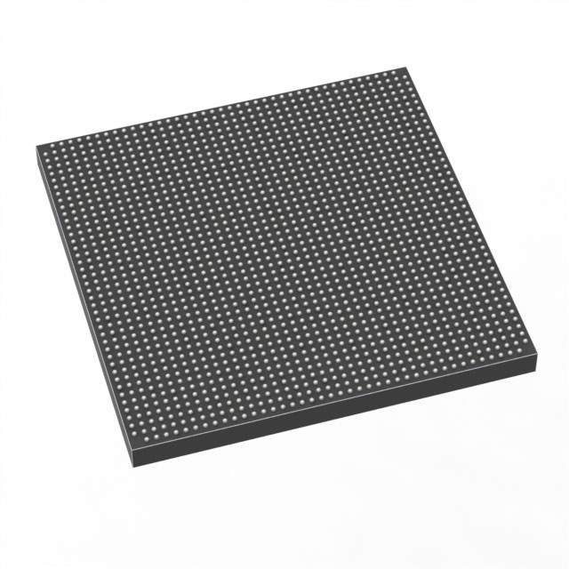
Overview of 1ST280EU1F50E1VG – Stratix® 10 TX FPGA, 2,800,000 logic elements, 440 I/O, 2397-BBGA
The 1ST280EU1F50E1VG is an Intel Stratix 10 TX field-programmable gate array supplied in a 2397-BBGA (FCBGA) package. It integrates a high-performance HyperFlex® core architecture with the Stratix 10 TX family’s advanced transceiver and I/O capabilities to address designs that require large programmable logic capacity and high aggregate bandwidth.
Targeted at high-speed communications, networking, and bandwidth-intensive system designs, this device delivers 2,800,000 logic elements, extensive on-chip RAM, and multi-gigabit transceiver capability as part of the Stratix 10 TX device family feature set.
Key Features
- Core Architecture HyperFlex® core architecture (Stratix 10 TX family) delivering the high-performance programmable fabric implemented in Intel 14 nm process; device-level logic capacity: 2,800,000 logic elements.
- On-chip Memory Large internal memory resources totaling 240,123,904 bits of RAM to support buffering, packet processing, and large on-chip data structures.
- High-speed Transceivers Stratix 10 TX family dual-mode transceivers supporting up to 57.8 Gbps PAM4 and 28.9 Gbps NRZ operation for chip-to-chip, chip-to-module, and backplane links.
- Hard IP Interfaces Family-level hardened IP options include PCI Express Gen3 and 10/25/100 Gbps Ethernet MACs with Reed–Solomon FEC support for NRZ and PAM4 signals (as documented for Stratix 10 TX devices).
- I/O and Package 440 general-purpose I/O lines in a 2397-BBGA FCBGA package (supplier device package: 2397-FBGA, FC 50×50), optimized for high-density board-level routing.
- Power and Supply Supported core supply range specified at 770 mV to 970 mV, enabling operation within the device’s defined power envelope.
- Operating Conditions Extended-grade device with an operating temperature range of 0°C to 100°C and RoHS compliance.
Typical Applications
- High-speed Networking and Switches On-chip capacity and high-rate transceivers support packet processing, MAC offload, and aggregation for switch and router line cards.
- Telecom and Optical Transport Dual-mode transceivers and hardened Ethernet/FEC IP make the device suitable for backplane or module interfaces in transport equipment.
- Data Center Interconnect Large logic and RAM resources enable complex acceleration, packet telemetry, and high-bandwidth interconnect functions.
- High-performance Compute Interfaces PCI Express Gen3 hard IP (documented for the family) and dense I/O allow integration into accelerator boards and host interfaces.
Unique Advantages
- Massive Logic Capacity: 2,800,000 logic elements provide headroom for large, complex designs and multi-function systems on a single device.
- High On-Chip Memory: 240,123,904 bits of RAM reduce external memory dependence for high-throughput buffering and state storage.
- High-bandwidth SerDes: Dual-mode transceiver capability (PAM4 and NRZ up to the documented family rates) supports flexible link architectures across applications.
- Dense I/O in a FCBGA Package: 440 I/O pins in a 2397-BBGA package simplify board routing for multi-channel systems and module interfaces.
- Designed for Extended-temperature Operation: 0°C to 100°C operating range supports deployment in a broad set of commercial and telecom environments.
- Regulatory Compliance: RoHS-compliant to meet environmental material requirements.
Why Choose 1ST280EU1F50E1VG?
1ST280EU1F50E1VG positions itself where large programmable capacity, extensive on-chip memory, and high-speed serial connectivity are required. With 2.8 million logic elements, nearly 240 million bits of RAM, and the Stratix 10 TX family’s transceiver and hardened interface capabilities, this device is suited for designs that consolidate complex packet-processing, routing, and high-bandwidth interconnect functions onto a single FPGA.
Choose this device when you need a scalable, high-capacity programmable fabric in a high-density package with defined supply and temperature ranges—enabling integration of feature-rich, bandwidth-critical systems while minimizing external component count.
Request a quote or submit an inquiry for part number 1ST280EU1F50E1VG to evaluate it for your next high-performance FPGA design.


Date Founded: 1968
Headquarters: Santa Clara, California, USA
Employees: 130,000+
Revenue: $54.23 Billion
Certifications and Memberships: ISO9001:2015, ISO14001:2015, ISO17025:2017, ISO27001:2022, ISO45001:2018, ISO50001:2018


