
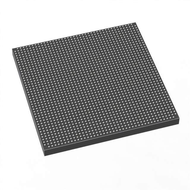
1ST280EU1F50I1VG
| Part Description |
Stratix® 10 TX Field Programmable Gate Array (FPGA) IC 440 2800000 2397-BBGA, FCBGA |
|---|---|
| Quantity | 558 Available (as of June 15, 2026) |

| Product Category | Field Programmable Gate Array (FPGA) |
|---|---|
| Manufacturer | Intel |
| Manufacturing Status | Active |
| Manufacturer Standard Lead Time | 12 Weeks |
| Datasheet |
Specifications & Environmental
| Device Package | 2397-FBGA, FC (50x50) | Grade | Industrial | Operating Temperature | -40°C – 100°C | ||
|---|---|---|---|---|---|---|---|
| Package / Case | 2397-BBGA, FCBGA | Number of I/O | 440 | Voltage | 770 mV - 970 mV | ||
| Mounting Method | Surface Mount | RoHS Compliance | Unknown | REACH Compliance | REACH Unaffected | ||
| Moisture Sensitivity Level | 3 (168 Hours) | Number of LABs/CLBs | 350000 | Number of Logic Elements/Cells | 2800000 | ||
| Number of Gates | N/A | ECCN | N/A | HTS Code | N/A | ||
| Qualification | N/A | Total RAM Bits | 240123904 |
Overview of 1ST280EU1F50I1VG – Stratix® 10 TX FPGA, 2.8M logic elements, 440 I/O, 2397-BBGA (FCBGA)
The 1ST280EU1F50I1VG is an Intel Stratix® 10 TX field programmable gate array (FPGA) packaged in a 2397-BBGA FCBGA. It pairs a high-density monolithic core fabric with advanced, dual-mode high-speed transceivers and hardened protocol IP to target demanding, high-bandwidth systems.
Designed for industrial-grade applications, this device delivers large programmable logic capacity, extensive on-chip memory, and a high I/O count—making it suitable for next-generation communications, networking, and compute acceleration designs that require high aggregate bandwidth and integration.
Key Features
- Core Architecture Intel HyperFlex® core architecture implemented in 14 nm tri-gate (FinFET) process with a monolithic fabric delivering 2,800,000 logic elements.
- High-speed Transceivers Dual-mode transceivers capable of 57.8 Gbps PAM4 and 28.9 Gbps NRZ operation; heterogeneous 3D SiP transceiver tiles enable high channel counts and flexible signal interfaces.
- Hardened Protocol IP Includes hardened PCI Express Gen3 and 10/25/100 Gbps Ethernet MAC IP with dedicated Reed–Solomon FEC for selected signal modes, reducing the need for external PHYs and offload logic.
- On-chip Memory Total RAM of 240,123,904 bits, with internal M20K SRAM blocks and select devices offering embedded eSRAM (47.25 Mbit) for large buffering and in-hardware data storage.
- DSP and Processing Hardened floating-point variable-precision DSP blocks and, in select devices, an embedded quad-core 64-bit Arm Cortex‑A53 Hard Processor System (HPS) for application-class processing.
- I/O and Package 440 I/O pins in a 2397-BBGA (50 × 50) FCBGA package; surface-mount mounting type suited for high-density board implementations.
- Power and Thermal Core voltage supply range of 770 mV to 970 mV and industrial operating temperature range from −40 °C to 100 °C.
- Configuration, Security, and Reliability Supports secure device management and configuration features, as well as SEU error detection and correction mechanisms to improve system reliability.
Typical Applications
- High-bandwidth Networking and Switching Used to implement switch fabrics, line cards, and backplane interfaces that require aggregated multi-terabit throughput and low-latency packet processing.
- Data Center Accelerators Suitable for compute acceleration and custom offload engines that leverage large logic capacity, DSP blocks, and on-chip memory for workload-specific processing.
- Telecommunications and Optical Transport Adaptable to PAM4/NRZ transceiver requirements for optical modules, chip-to-module, and chip-to-chip interconnects with integrated FEC and MAC IP.
- High-speed Serial I/O Systems Ideal for designs requiring many high-rate serial channels and robust protocol support such as PCIe and multi-rate Ethernet links.
Unique Advantages
- Highly Integrated Fabric: 2.8 million logic elements and large on-chip RAM reduce external logic and memory needs, simplifying BOM and board complexity.
- Flexible High-speed I/O: Dual-mode transceivers and up to hundreds of transceiver channels support a wide range of serial link topologies and data rates for modular system design.
- Hardened IP Blocks: Built-in PCIe Gen3 and multi-rate Ethernet MAC with FEC lower development time and provide proven protocol handling in hardware.
- Industrial Temperature Range: Rated from −40 °C to 100 °C to meet industrial deployment conditions without derating core specifications.
- Advanced Packaging and Interconnect: Heterogeneous 3D SiP and EMIB-based packaging concepts (described for the family) support dense integration of fabric and transceiver tiles.
- On-chip Processing Options: Availability of an embedded quad-core Arm Cortex‑A53 HPS in select devices enables tighter hardware/software partitioning and reduced external processor requirements.
Why Choose 1ST280EU1F50I1VG?
The 1ST280EU1F50I1VG delivers a combination of very high logic density, extensive on-chip memory, and robust high-speed transceivers in an industrial-grade Stratix 10 TX package. Its architecture and hardened protocol IP make it a strong candidate for designers targeting high-bandwidth communications, data center acceleration, and advanced serial I/O systems that require integrated handling of complex protocols.
Choosing this device provides a path to scalable, high-performance system designs with features intended to reduce external components and accelerate development—backed by the Stratix 10 TX device family documentation and configuration/security capabilities described in the product literature.
Request a quote or submit an inquiry to obtain pricing, lead time, and availability for the 1ST280EU1F50I1VG.


Date Founded: 1968
Headquarters: Santa Clara, California, USA
Employees: 130,000+
Revenue: $54.23 Billion
Certifications and Memberships: ISO9001:2015, ISO14001:2015, ISO17025:2017, ISO27001:2022, ISO45001:2018, ISO50001:2018


