
1ST280EY1F55E2VG
| Part Description |
Stratix® 10 TX Field Programmable Gate Array (FPGA) IC 296 2800000 2912-BBGA, FCBGA |
|---|---|
| Quantity | 1,050 Available (as of June 15, 2026) |
| Product Category | Field Programmable Gate Array (FPGA) |
|---|---|
| Manufacturer | Intel |
| Manufacturing Status | Active |
| Manufacturer Standard Lead Time | 12 Weeks |
| Datasheet |
Specifications & Environmental
| Device Package | 2912-FBGA, FC (55x55) | Grade | Extended | Operating Temperature | 0°C – 100°C | ||
|---|---|---|---|---|---|---|---|
| Package / Case | 2912-BBGA, FCBGA | Number of I/O | 296 | Voltage | 770 mV - 970 mV | ||
| Mounting Method | Surface Mount | RoHS Compliance | Unknown | REACH Compliance | REACH Unaffected | ||
| Moisture Sensitivity Level | 3 (168 Hours) | Number of LABs/CLBs | 350000 | Number of Logic Elements/Cells | 2800000 | ||
| Number of Gates | N/A | ECCN | N/A | HTS Code | N/A | ||
| Qualification | N/A | Total RAM Bits | 240123904 |
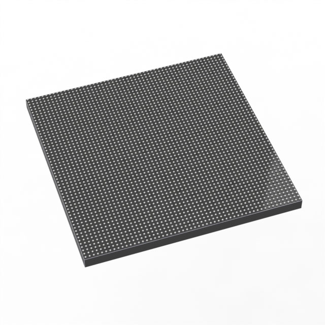
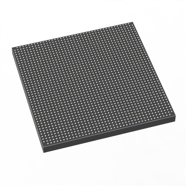
Overview of 1ST280EY1F55E2VG – Stratix® 10 TX FPGA, 2912-BBGA
The 1ST280EY1F55E2VG is an Intel Stratix® 10 TX field programmable gate array (FPGA) in a 2912-ball FCBGA package. It implements the Intel HyperFlex® core architecture and high-speed transceiver technology to address designs that require very large logic capacity, extensive on-chip memory, and multi‑Gb/s serial connectivity.
Targeted at high-bandwidth and high-performance applications, this device combines up to 2,800,000 logic elements and 240,123,904 bits of internal RAM with dual‑mode transceivers and hardened networking and PCI Express IP to enable chip-to-chip, chip-to-module, and backplane system designs.
Key Features
- Core and Architecture Intel HyperFlex® core architecture implemented on Intel 14 nm tri‑gate (FinFET) technology, delivering the device’s high logic capacity of 2,800,000 logic elements.
- High-Speed Transceivers Dual‑mode transceivers capable of 57.8 Gbps PAM4 and 28.9 Gbps NRZ operation; architecture supports up to 144 full‑duplex transceiver channels for demanding serial bandwidth needs and multi‑lane links.
- On-Chip Memory Large internal RAM totaling 240,123,904 bits to support buffering, packet processing, and large-scale logic designs.
- Hardened IP Integrated hardened PCI Express Gen3 and 10/25/100 Gbps Ethernet MAC blocks with dedicated FEC capabilities for NRZ and PAM4 signaling to simplify high‑speed protocol integration.
- I/O and Package 296 general-purpose I/O pins in a 2912-ball BGA (FCBGA) package; supplier package specified as 2912-FBGA, FC (55×55 mm) for compact, surface-mount system integration.
- Power and Operating Range Core supply range specified at 770 mV to 970 mV; operating temperature range 0°C to 100°C and RoHS compliant.
- Advanced Packaging Heterogeneous 3D System-in-Package (SiP) and EMIB packaging techniques documented in the Stratix 10 TX family for combining high-speed transceiver tiles with the monolithic core fabric.
Typical Applications
- High-Speed Networking and Switching Implements multi‑Tbps datapaths and 10/25/100 Gbps Ethernet MACs for line cards, switches, and routers requiring high aggregate bandwidth.
- Backplane and Chip-to-Chip Links Dual‑mode transceivers and support for PAM4/NRZ signaling enable use in high-density backplane fabrics and chip-to‑chip or module interconnects.
- PCI Express Interfaces and Accelerators Hardened PCIe Gen3 IP supports integration of host interfaces and acceleration functions in compute and storage platforms.
- Custom High‑Performance Logic Large logic element count and substantial on‑chip RAM make the device suitable for packet processing, signal processing, and complex system controllers.
Unique Advantages
- High Logic Capacity: 2,800,000 logic elements provide substantial room for large-scale, multi-function FPGA implementations.
- Flexible High-Speed I/O: Dual‑mode 57.8 Gbps PAM4 / 28.9 Gbps NRZ transceivers and up to 144 full‑duplex channels support a wide range of serial link topologies.
- Built‑In Protocol Support: Hardened PCIe Gen3 and 10/25/100 Gbps Ethernet MAC blocks reduce integration time for networking and host-interface designs.
- Significant On-Chip Memory: 240,123,904 bits of internal RAM to support buffering, packet handling, and large processing data sets without immediate external memory dependence.
- Robust Packaging and I/O Count: 2912‑ball FCBGA package with 296 I/O pins balances high connectivity with a compact surface‑mount footprint.
- Compliance and Grade: RoHS compliant and specified for extended‑grade operation from 0°C to 100°C for applications requiring that temperature range.
Why Choose 1ST280EY1F55E2VG?
The 1ST280EY1F55E2VG positions itself for systems that demand very high logic density, extensive internal memory, and broad high‑speed serial connectivity. Its HyperFlex core architecture, large logic element count, and dual‑mode transceivers enable designs that need both programmable logic scale and multi‑Gb/s link performance.
This device is suited for engineering teams designing next‑generation networking, backplane, and accelerator platforms where integrated hardened protocol IP, high aggregate bandwidth, and compact FCBGA packaging contribute to reduced system complexity and faster time to market.
Request a quote or submit an inquiry to our sales team to discuss availability, lead times, and pricing for the 1ST280EY1F55E2VG Stratix® 10 TX FPGA.


Date Founded: 1968
Headquarters: Santa Clara, California, USA
Employees: 130,000+
Revenue: $54.23 Billion
Certifications and Memberships: ISO9001:2015, ISO14001:2015, ISO17025:2017, ISO27001:2022, ISO45001:2018, ISO50001:2018


