
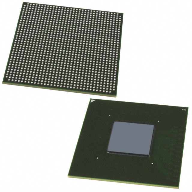
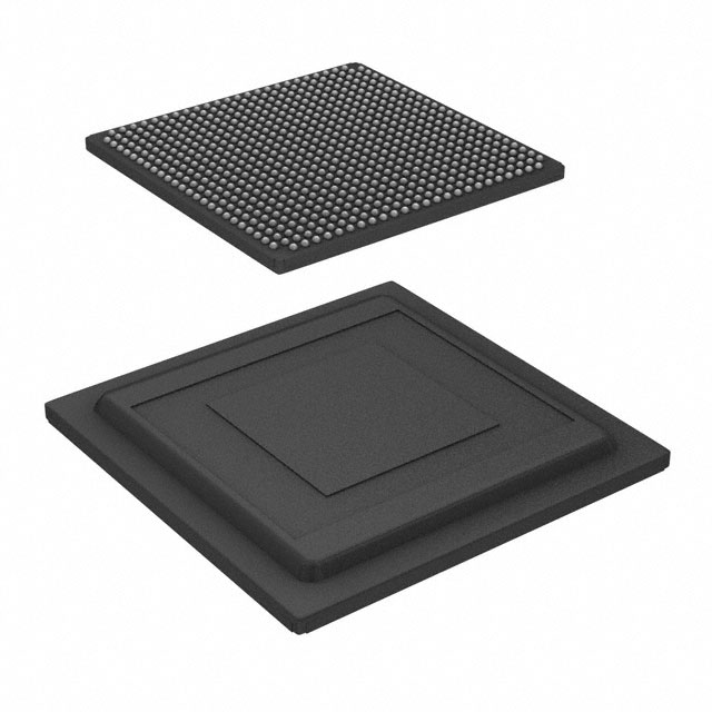
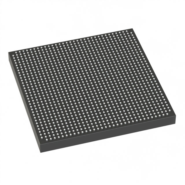
5AGXMA7D4F27C5G
| Part Description |
Arria V GX Field Programmable Gate Array (FPGA) IC 336 15470592 242000 672-BBGA, FCBGA |
|---|---|
| Quantity | 1,023 Available (as of June 15, 2026) |

| Product Category | Field Programmable Gate Array (FPGA) |
|---|---|
| Manufacturer | Intel |
| Manufacturing Status | Active |
| Manufacturer Standard Lead Time | 12 Weeks |
| Datasheet |
Specifications & Environmental
| Device Package | 672-FBGA (27x27) | Grade | Commercial | Operating Temperature | 0°C – 85°C | ||
|---|---|---|---|---|---|---|---|
| Package / Case | 672-BBGA, FCBGA | Number of I/O | 336 | Voltage | 1.07 V - 1.13 V | ||
| Mounting Method | Surface Mount | RoHS Compliance | RoHS Compliant | REACH Compliance | REACH Unaffected | ||
| Moisture Sensitivity Level | 3 (168 Hours) | Number of LABs/CLBs | 11460 | Number of Logic Elements/Cells | 242000 | ||
| Number of Gates | N/A | ECCN | PENDING ECCN | HTS Code | 0000.00.0000 | ||
| Qualification | N/A | Total RAM Bits | 15470592 |
Overview of 5AGXMA7D4F27C5G – Arria V GX Field Programmable Gate Array (FPGA) IC 336 15470592 242000 672-BBGA, FCBGA
The 5AGXMA7D4F27C5G is an Intel Arria V GX Field Programmable Gate Array (FPGA) supplied in a 672-ball FCBGA package. It provides a large logic fabric, substantial on-chip RAM, and a broad I/O complement for designs that require significant programmable logic, embedded memory, and flexible interfacing in a commercial-grade, surface-mount package.
Key architectural facts for system design include 242,000 logic elements, approximately 15.47 Mbits of embedded memory, and 336 user I/O pins. The device operates from a core supply range of 1.07 V to 1.13 V and is rated for commercial operating temperatures (0 °C to 85 °C).
Key Features
- Logic Capacity 242,000 logic elements for implementing complex custom logic, datapaths, and state machines.
- Embedded Memory Approximately 15.47 Mbits of on-chip RAM to support buffering, FIFOs, and memory-mapped logic resources.
- I/O Resources 336 user I/O pins to support extensive peripheral connectivity and board-level interfacing.
- Package and Mounting 672-ball FCBGA (672-FBGA, 27 × 27) surface-mount package for high-density board integration.
- Power and Voltage Core voltage supply specified between 1.07 V and 1.13 V to guide power-supply design and sequencing.
- Operating Range Commercial grade device rated for 0 °C to 85 °C operation.
- Compliance RoHS-compliant for regulatory and manufacturing alignment.
- Manufacturer Intel (Arria V GX family) with an available device datasheet covering electrical characteristics and configuration specifications.
Typical Applications
- Custom Logic and Prototyping Implement high-density custom logic functions and prototypes that require up to 242,000 logic elements and significant embedded memory.
- Memory-Intensive Processing On-chip RAM (≈15.47 Mbits) supports buffering, packet storage, and intermediate data structures without immediate external memory dependence.
- High-Connectivity Systems Leverage 336 I/O pins to interface with multiple peripherals, sensors, or board-level buses in compact system designs.
Unique Advantages
- Substantial Logic Density: 242,000 logic elements enable integration of complex state machines, datapaths, and custom accelerators on a single device, reducing component count.
- On-Chip Memory Resources: Approximately 15.47 Mbits of embedded RAM reduce dependence on external memory for many buffering and caching needs, simplifying PCB layout and BOM.
- Generous I/O Count: 336 user I/O pins provide flexibility for multi-channel interfaces, control signals, and parallel connectivity without additional multiplexing hardware.
- Compact Package Footprint: 672-ball FCBGA (27 × 27) surface-mount package supports high-density board designs while maintaining robust signal routing options.
- Commercial Temperature Rating: Specified 0 °C to 85 °C range aligns with a wide set of commercial and enterprise applications and deployments.
- Regulatory Compliance: RoHS compliance supports environmentally conscious manufacturing and supply-chain requirements.
Why Choose 5AGXMA7D4F27C5G?
The 5AGXMA7D4F27C5G Arria V GX FPGA combines a large logic fabric, substantial embedded memory, and a high I/O count in a commercial-grade FCBGA package. These measurable capabilities make it well suited for system designs that require dense programmable logic, on-chip data storage, and broad interfacing while maintaining a compact PCB footprint.
For design teams that prioritize integration, predictable electrical characteristics, and vendor-backed documentation, this device provides a clear set of specifications to guide power, thermal, and I/O planning. Detailed electrical and configuration parameters are documented in the Arria V device datasheet for engineering validation and system integration.
Request a quote or submit an inquiry for part number 5AGXMA7D4F27C5G to check pricing, availability, and lead time for your next design.


Date Founded: 1968
Headquarters: Santa Clara, California, USA
Employees: 130,000+
Revenue: $54.23 Billion
Certifications and Memberships: ISO9001:2015, ISO14001:2015, ISO17025:2017, ISO27001:2022, ISO45001:2018, ISO50001:2018


