
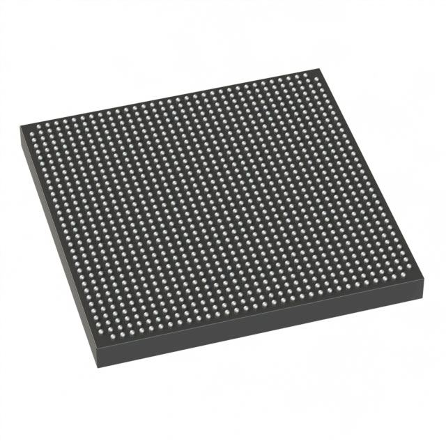
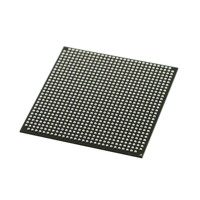
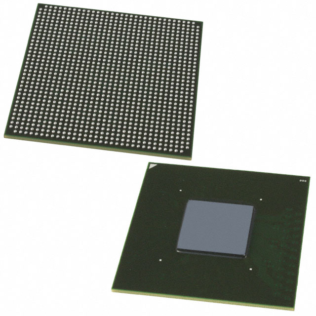
5AGXMB3G4F35C4G
| Part Description |
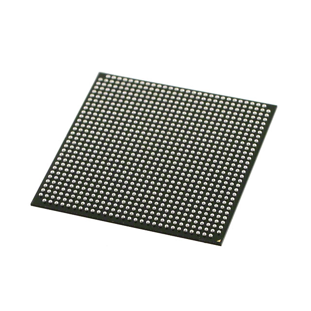
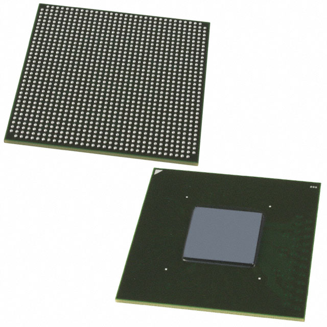
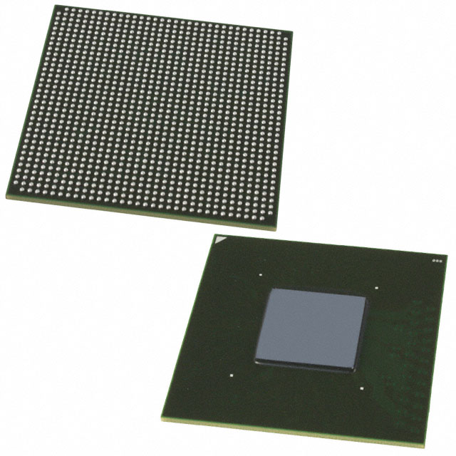
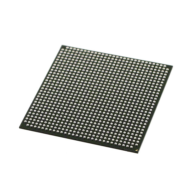
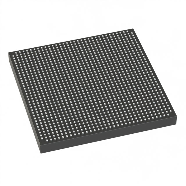
Arria V GX Field Programmable Gate Array (FPGA) IC 544 19822592 362000 1152-BBGA, FCBGA |
|---|---|
| Quantity | 224 Available (as of October 8, 2026) |
| Product Category | Field Programmable Gate Array (FPGA) |
|---|---|
| Manufacturer | Intel |
| Manufacturing Status | Active |
| Manufacturer Standard Lead Time | 12 Weeks |
| Datasheet |
Specifications & Environmental
| Device Package | 1152-FBGA, FC (35x35) | Grade | Commercial | Operating Temperature | 0°C – 85°C | ||
|---|---|---|---|---|---|---|---|
| Package / Case | 1152-BBGA, FCBGA | Number of I/O | 544 | Voltage | 1.07 V - 1.13 V | ||
| Mounting Method | Surface Mount | RoHS Compliance | RoHS Compliant | REACH Compliance | REACH Unaffected | ||
| Moisture Sensitivity Level | 3 (168 Hours) | Number of LABs/CLBs | 17110 | Number of Logic Elements/Cells | 362000 | ||
| Number of Gates | N/A | ECCN | PENDING ECCN | HTS Code | 0000.00.0000 | ||
| Qualification | N/A | Total RAM Bits | 19822592 |
Overview of 5AGXMB3G4F35C4G – Arria V GX Field Programmable Gate Array (FPGA) IC
The 5AGXMB3G4F35C4G is an Intel Arria V GX family FPGA offered in a commercial grade package. It provides a high logic capacity architecture with 362,000 logic elements and approximately 19.8 Mbits of on‑chip RAM, paired with a large 544‑pin I/O resource set. The device is supplied in a 1152‑FBGA (35 × 35 mm) FCBGA package and operates within a core voltage range of 1.07 V to 1.13 V and an ambient temperature range of 0 °C to 85 °C.
Key Features
- Core Logic Capacity 362,000 logic elements to support complex, high‑density logic implementations.
- Embedded Memory Approximately 19.8 Mbits of on‑chip RAM for buffering, state storage, and memory‑intensive functions.
- High I/O Count 544 user I/O pins to accommodate extensive peripheral interfaces and board‑level connectivity.
- Package 1152‑FBGA, FCBGA (35 × 35 mm) footprint for a compact board layout while supporting many I/Os.
- Power and Supply Defined core supply range of 1.07 V to 1.13 V for predictable power design and rail budgeting.
- Operating Range Commercial grade operation from 0 °C to 85 °C for standard embedded and system applications.
- Standards Compliance RoHS compliant.
Typical Applications
- High‑density custom logic designs Suitable where up to 362,000 logic elements are required to implement complex finite state machines, custom datapaths, or protocol engines.
- Memory‑intensive functions Use the approximately 19.8 Mbits of embedded RAM for packet buffering, lookup tables, or on‑chip storage to reduce external memory dependence.
- Multi‑interface systems The 544 I/O pins support designs that require many simultaneous external connections, parallel buses, or multiple peripheral interfaces.
Unique Advantages
- High logic density: 362,000 logic elements enable consolidation of multiple functions into a single FPGA, reducing system BOM and board area.
- Substantial on‑chip memory: Approximately 19.8 Mbits of embedded RAM supports larger on‑chip buffers and state storage, improving deterministic behavior.
- Extensive I/O resources: 544 I/Os provide flexibility for interfacing to sensors, buses, and peripherals without immediate need for external GPIO expanders.
- Compact BGA package: 1152‑FBGA (35 × 35 mm) helps contain solution size while supporting a high pin count for dense system designs.
- Commercial operating range: 0 °C to 85 °C aligns with typical commercial embedded system environments and simplifies thermal planning.
- RoHS compliance: Meets regulatory requirements for lead‑free manufacturing flows.
Why Choose 5AGXMB3G4F35C4G?
The 5AGXMB3G4F35C4G Arria V GX FPGA combines a large logic fabric, significant on‑chip RAM, and a high I/O count in a compact 1152‑FBGA package. Its defined core voltage range and commercial temperature rating make it suitable for mainstream embedded and system designs that need high logic and memory capacity without relying on external resources. The Arria V family datasheet and device specifications provide the electrical and configuration details necessary for integration into professional designs.
Engineers and procurement teams looking for a high‑capacity, commercial‑grade FPGA with extensive I/O and embedded memory will find this device well suited to consolidate functionality and streamline board-level integration.
Request a quote or submit a purchase inquiry to obtain pricing, availability, and lead‑time information for 5AGXMB3G4F35C4G.





















Date Founded: 1968
Headquarters: Santa Clara, California, USA
Employees: 130,000+
Revenue: $54.23 Billion
Certifications and Memberships: ISO9001:2015, ISO14001:2015, ISO17025:2017, ISO27001:2022, ISO45001:2018, ISO50001:2018


