
5AGXMB3G4F35C4N
| Part Description |
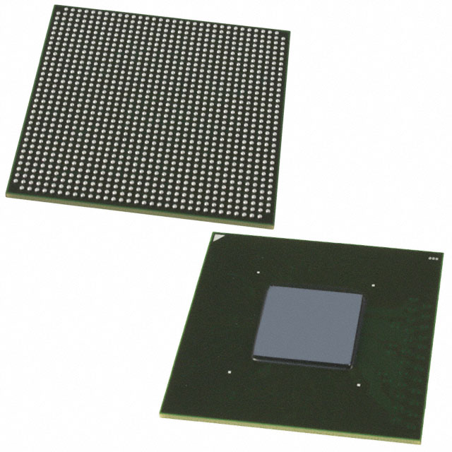
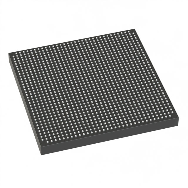
Arria V GX Field Programmable Gate Array (FPGA) IC 544 19822592 362000 1152-BBGA, FCBGA Exposed Pad |
|---|---|
| Quantity | 662 Available (as of October 7, 2026) |
| Product Category | Field Programmable Gate Array (FPGA) |
|---|---|
| Manufacturer | Intel |
| Manufacturing Status | Obsolete |
| Manufacturer Standard Lead Time | Contact Us |
| Datasheet |
Specifications & Environmental
| Device Package | 1152-FBGA (35x35) | Grade | Commercial | Operating Temperature | 0°C – 85°C | ||
|---|---|---|---|---|---|---|---|
| Package / Case | 1152-BBGA, FCBGA Exposed Pad | Number of I/O | 544 | Voltage | 1.07 V - 1.13 V | ||
| Mounting Method | Surface Mount | RoHS Compliance | RoHS Compliant | REACH Compliance | REACH Unknown | ||
| Moisture Sensitivity Level | 3 (168 Hours) | Number of LABs/CLBs | 17110 | Number of Logic Elements/Cells | 362000 | ||
| Number of Gates | N/A | ECCN | 3A001A2C | HTS Code | 8542.39.0001 | ||
| Qualification | N/A | Total RAM Bits | 19822592 |
Overview of 5AGXMB3G4F35C4N – Arria V GX Field Programmable Gate Array (FPGA) IC, 544 I/O, 1152‑BBGA
The 5AGXMB3G4F35C4N is an Arria V GX field programmable gate array (FPGA) in a surface‑mount FCBGA package designed for commercial applications. The device provides substantial on‑chip programmable logic and embedded memory alongside a high I/O count and a compact 1152‑BBGA package for board‑level integration.
On‑chip resources include approximately 362,000 logic elements and approximately 19.8 Mbits of embedded RAM, with a core supply range of 1.07 V to 1.13 V and a commercial operating temperature range of 0 °C to 85 °C. The Arria V device family datasheet documents electrical, switching, configuration, and I/O timing specifications in detail for system design and validation.
Key Features
- Core Logic Approximately 362,000 logic elements to implement large-scale programmable logic and custom hardware functions.
- Embedded Memory Approximately 19.8 Mbits of on‑chip RAM to support buffering, state storage, and data‑intensive processing.
- I/O Density 544 general-purpose I/O pins to accommodate complex board‑level interfacing and multiple peripheral connections.
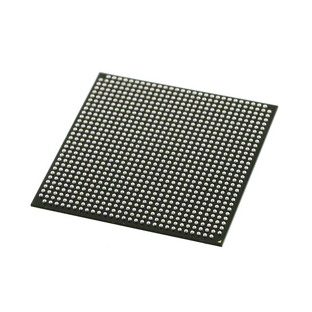
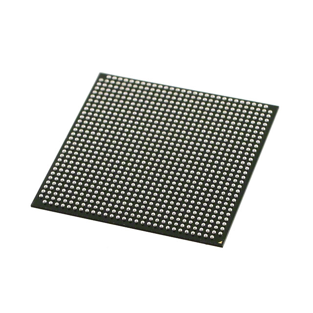
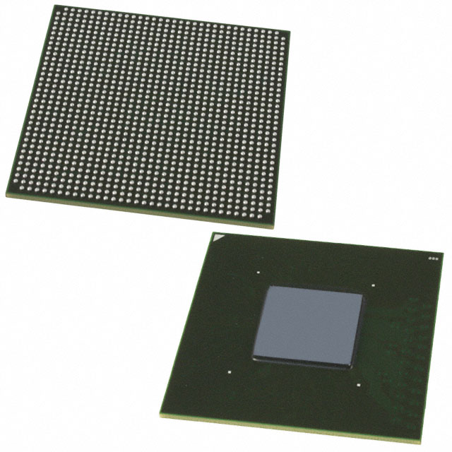
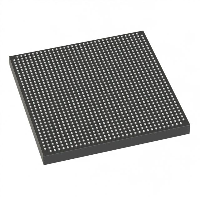
- Package & Mounting 1152‑BBGA, FCBGA exposed pad package (supplier package: 1152‑FBGA, 35×35) optimized for surface‑mount assembly and thermal management via the exposed pad.
- Power Specified core voltage supply range of 1.07 V to 1.13 V for regulated power‑rail design.
- Operating Grade & Temperature Commercial grade device rated for operation from 0 °C to 85 °C.
- Compliance RoHS compliant.
- Documentation Arria V device datasheet provides comprehensive electrical characteristics, switching behavior, configuration specifications, and I/O timing for system design.
Typical Applications
- FPGA‑based custom logic Leverage the large logic element count and embedded RAM to implement custom state machines, data path acceleration, and protocol logic.
- High‑density I/O systems Use the 544 I/O pins for multi‑channel interfacing, board aggregation, and complex peripheral connectivity.
- Embedded system integration Compact FCBGA package and exposed pad simplify board layout and thermal considerations for compact commercial designs.
Unique Advantages
- High logic capacity: Approximately 362,000 logic elements provide the silicon scale needed for complex programmable designs without external logic expansion.
- Substantial on‑chip RAM: Approximately 19.8 Mbits of embedded memory reduces dependence on external memory for buffering and local data storage.
- Extensive I/O support: 544 I/O pins enable dense peripheral connectivity and flexible system partitioning.
- Board‑friendly package: 1152‑BBGA (35×35) FCBGA with exposed pad supports surface‑mount assembly and improved thermal path through the PCB.
- Defined power envelope: Narrow core voltage specification (1.07 V–1.13 V) simplifies power supply design and regulation planning.
- Commercial readiness: Rated for 0 °C to 85 °C operation and RoHS compliant for mainstream commercial product deployment.
Why Choose 5AGXMB3G4F35C4N?
The 5AGXMB3G4F35C4N Arria V GX FPGA positions itself for commercial designs that require a combination of large programmable logic capacity, significant embedded RAM, and a high I/O count in a compact BGA package. Its defined core voltage range and surface‑mount FCBGA footprint make it suitable for tightly integrated boards where package density and thermal management are considerations.
This part is suited to engineering teams building complex programmable systems that benefit from on‑chip memory and plentiful I/O while relying on the Arria V device family documentation for electrical, configuration, and timing guidance during design and validation.
Request a quote or submit a request for pricing and availability to move your design forward.





















Date Founded: 1968
Headquarters: Santa Clara, California, USA
Employees: 130,000+
Revenue: $54.23 Billion
Certifications and Memberships: ISO9001:2015, ISO14001:2015, ISO17025:2017, ISO27001:2022, ISO45001:2018, ISO50001:2018


