
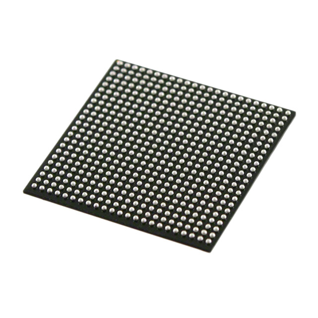
5CGXFC5C7U19C8N
| Part Description |
Cyclone® V GX Field Programmable Gate Array (FPGA) IC 224 5001216 77000 484-FBGA |
|---|---|
| Quantity | 973 Available (as of October 8, 2026) |
| Product Category | Field Programmable Gate Array (FPGA) |
|---|---|
| Manufacturer | Intel |
| Manufacturing Status | Active |
| Manufacturer Standard Lead Time | 12 Weeks |
| Datasheet |
Specifications & Environmental
| Device Package | 484-UBGA (19x19) | Grade | Commercial | Operating Temperature | 0°C – 85°C | ||
|---|---|---|---|---|---|---|---|
| Package / Case | 484-FBGA | Number of I/O | 224 | Voltage | 1.07 V - 1.13 V | ||
| Mounting Method | Surface Mount | RoHS Compliance | RoHS Compliant | REACH Compliance | REACH Unaffected | ||
| Moisture Sensitivity Level | 3 (168 Hours) | Number of LABs/CLBs | 29080 | Number of Logic Elements/Cells | 77000 | ||
| Number of Gates | N/A | ECCN | 3A991D | HTS Code | 8542.39.0001 | ||
| Qualification | N/A | Total RAM Bits | 5001216 |
Overview of 5CGXFC5C7U19C8N – Cyclone® V GX FPGA, 484‑FBGA, 77,000 logic elements
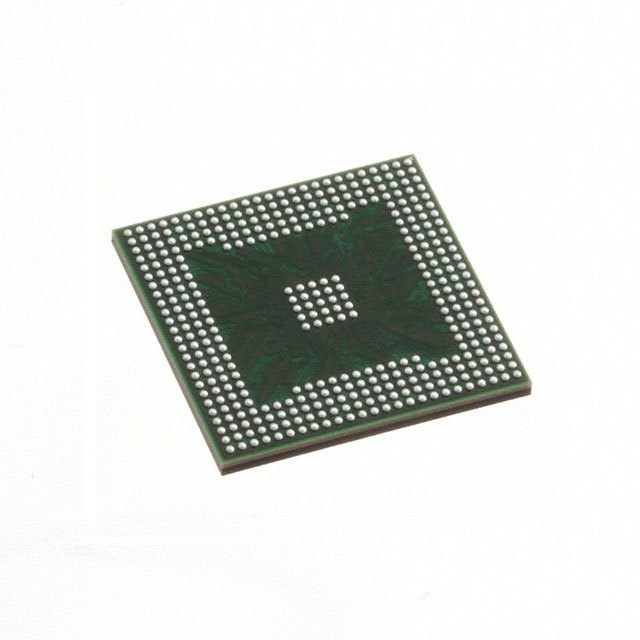
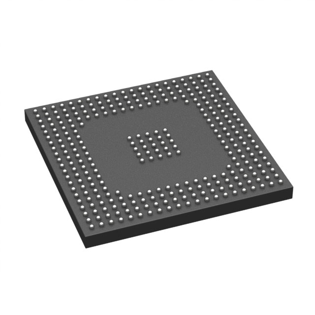
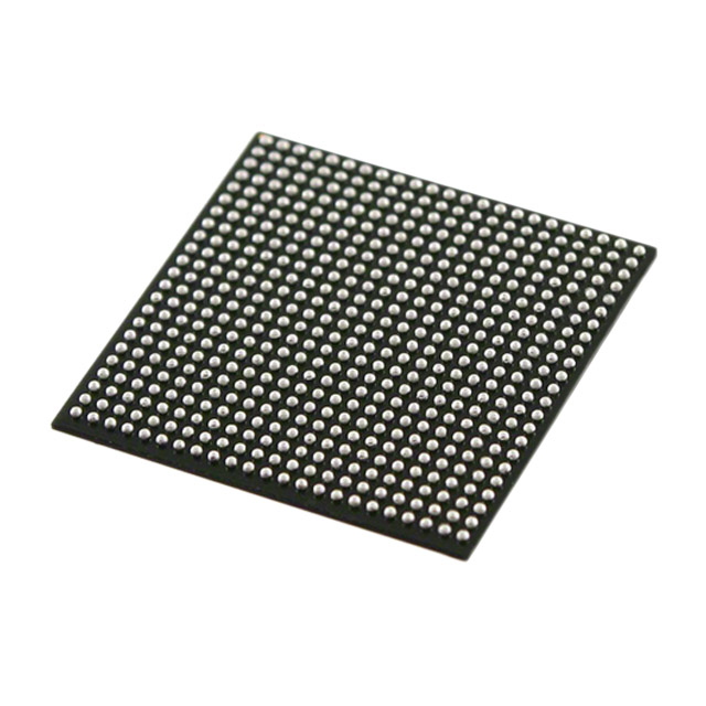
The 5CGXFC5C7U19C8N is an Intel Cyclone V GX field programmable gate array supplied in a 484‑FBGA (484‑UBGA, 19×19) package for surface‑mount assembly. This commercial‑grade FPGA integrates a large logic fabric, substantial on‑chip RAM, and I/O density to support embedded processing, high‑bandwidth interfaces, and DSP‑focused designs where power efficiency and integration matter.
As part of the Cyclone V family, the device leverages 28‑nm low‑power process technology and series‑level hard IP (including memory controllers and high‑speed transceivers) to address applications that require reduced power consumption, configurable logic capacity, and robust external memory and I/O support.
Key Features
- Logic Capacity — Provides 77,000 logic elements to implement complex state machines, datapaths, and control logic.
- Embedded Memory — Approximately 5.0 Mbits of on‑chip RAM (5,001,216 bits) for buffering, FIFOs, and local data storage.
- I/O Density — 224 general‑purpose I/O pins to interface with peripherals, memory devices, and front‑end systems.
- Power and Core Voltage — Operates with a core voltage supply range of 1.07 V to 1.13 V (nominal 1.1 V series architecture) to support low‑power designs.
- Package and Mounting — 484‑FBGA (supplier package 484‑UBGA, 19×19) optimized for surface‑mount assembly in high‑density boards.
- Operating Range — Commercial grade operation from 0 °C to 85 °C.
- Standards and Compliance — RoHS‑compliant construction for global manufacturing requirements.
- Series Features (Cyclone V) — Built on TSMC 28‑nm low‑power (28LP) process; series offers enhanced 8‑input adaptive logic modules, M10K memory blocks, variable‑precision DSP blocks, hard memory controllers, and integrated high‑speed transceivers.
Typical Applications
- Wireless and Wireline Communications — Implement protocol processing, framing, and interface bridging leveraging the device’s logic density, on‑chip RAM, and Cyclone V series transceiver support.
- Embedded SoC and HPS‑enabled Designs — Combine FPGA fabric with series hard IP to accelerate processor interfaces, memory controllers, and custom accelerators.
- DSP and Signal Processing — Use the logic fabric and embedded RAM for filtering, packet buffering, and variable‑precision DSP implementations described for the Cyclone V family.
- High‑Bandwidth External Memory Interfaces — Deploy the device where hard memory controllers and external memory performance are required for data buffering or system memory expansion.
Unique Advantages
- Substantial Logic and RAM in a Compact Package: 77,000 logic elements and ~5.0 Mbits of embedded memory provide a balance of compute and storage for mid‑range FPGA functions without large form factors.
- High I/O Count: 224 I/O pins enable rich peripheral connectivity and memory interface options while keeping board routing manageable in a 19×19 UBGA footprint.
- Low‑Power Process Technology: Built on a 28‑nm low‑power process with ~1.1 V core operation, helping designs meet tighter power budgets compared with older nodes.
- Series‑Level Integration: Access to Cyclone V family features such as hard memory controllers, variable‑precision DSP blocks, and high‑speed transceivers simplifies system partitioning between software and hardware.
- Commercial‑Grade Availability: Operates across a 0 °C to 85 °C range and is RoHS‑compliant for mainstream commercial production environments.
Why Choose 5CGXFC5C7U19C8N?
The 5CGXFC5C7U19C8N positions itself as a versatile, commercially graded Cyclone V GX FPGA that balances substantial logic capacity, embedded memory, and high I/O density in a compact 484‑FBGA package. It is suited for customers designing mid‑range embedded systems, communications interfaces, and DSP accelerators where power efficiency, series‑level hard IP, and predictable thermal/voltage operating windows are important.
Selecting this part provides a clear upgrade path within the Cyclone V family, leveraging the ecosystem and documentation associated with the series while delivering a practical mix of logic, RAM, and I/O for rapid prototyping through production runs.
Request a quote or submit a procurement inquiry for part number 5CGXFC5C7U19C8N to get pricing, availability, and lead‑time information.























Date Founded: 1968
Headquarters: Santa Clara, California, USA
Employees: 130,000+
Revenue: $54.23 Billion
Certifications and Memberships: ISO9001:2015, ISO14001:2015, ISO17025:2017, ISO27001:2022, ISO45001:2018, ISO50001:2018


