
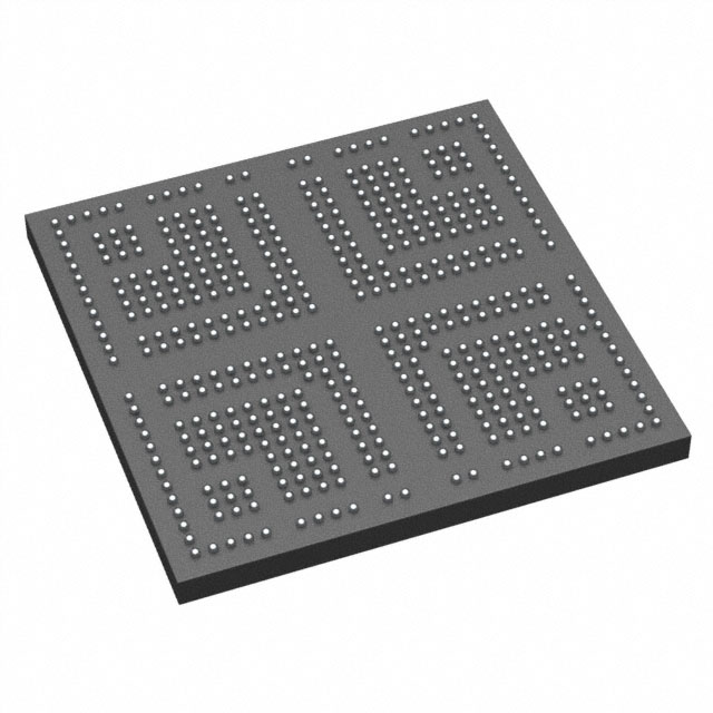
5CGXFC7C6F23C6N
| Part Description |
Cyclone® V GX Field Programmable Gate Array (FPGA) IC 240 7880704 149500 484-BGA |
|---|---|
| Quantity | 793 Available (as of June 10, 2026) |

| Product Category | Field Programmable Gate Array (FPGA) |
|---|---|
| Manufacturer | Intel |
| Manufacturing Status | Active |
| Manufacturer Standard Lead Time | 16 Weeks |
| Datasheet |
Specifications & Environmental
| Device Package | 484-FBGA (23x23) | Grade | Commercial | Operating Temperature | 0°C – 85°C | ||
|---|---|---|---|---|---|---|---|
| Package / Case | 484-BGA | Number of I/O | 240 | Voltage | 1.07 V - 1.13 V | ||
| Mounting Method | Surface Mount | RoHS Compliance | RoHS Compliant | REACH Compliance | REACH Unaffected | ||
| Moisture Sensitivity Level | 3 (168 Hours) | Number of LABs/CLBs | 56480 | Number of Logic Elements/Cells | 149500 | ||
| Number of Gates | N/A | ECCN | 3A991D | HTS Code | 8542.39.0001 | ||
| Qualification | N/A | Total RAM Bits | 7880704 |
Overview of 5CGXFC7C6F23C6N – Cyclone® V GX FPGA, 149,500 Logic Elements, 240 I/O, 484‑BGA
The 5CGXFC7C6F23C6N is an Intel Cyclone® V GX field-programmable gate array (FPGA) delivered in a 484‑ball BGA. It offers high logic capacity and on-chip RAM for mid- to high-density FPGA designs, with a 240‑pin I/O footprint and a 484‑FBGA (23×23) package for compact, high‑pin‑count applications.
As a member of the Cyclone V family, this device is built around low‑power silicon and family-level architectural elements intended for applications in industrial control, wireless/wireline infrastructure, and defense systems that require flexible programmable logic and embedded memory.
Key Features
- Logic Capacity Approximately 149,500 logic elements provide substantial programmable logic resources for complex control, signal processing, and glue‑logic implementations.
- Embedded Memory Approximately 7.88 Mbits of on‑chip RAM (total RAM bits: 7,880,704) to support buffering, frame storage, and local data structures without external memory for many use cases.
- I/O and Package 240 user I/O pins in a 484‑ball BGA footprint; supplier package listed as 484‑FBGA (23×23) with surface‑mount mounting for high‑density board designs.
- Power Supply Core supply range of 1.07 V to 1.13 V (family nominal core voltage documented as 1.1 V), enabling low‑voltage operation and power‑sensitive designs.
- Operating Range & Grade Commercial grade device specified for operation from 0 °C to 85 °C.
- Family-Level Architecture Part of the Cyclone V family, which includes enhanced adaptive logic modules, variable‑precision DSP resources, hard memory controllers, and integrated transceiver options as documented for the series.
- Compliance RoHS‑compliant for conformity with common lead‑free design and manufacturing requirements.
Typical Applications
- Industrial Control Programmable logic and on‑chip RAM support motor control, PLC interfaces, and real‑time protocol handling in factory automation and machine control systems.
- Wireless and Wireline Infrastructure Logic density and embedded memory enable packet handling, protocol bridging, and front‑end processing functions in base stations and network equipment.
- Signal Processing and Video Large logic element count and on‑chip RAM allow implementation of moderate‑complexity DSP pipelines, video pre‑processing, and frame buffering.
- Defense and Avionics Subsystems Flexible logic and I/O resources provide reconfigurable processing for communications, sensor fusion, and custom protocol interfaces.
Unique Advantages
- High Logic Density: The device’s ~149,500 logic elements let designers implement sizeable custom logic and state machines on a single FPGA.
- Substantial Embedded Memory: Approximately 7.88 Mbits of on‑chip RAM reduces dependence on external memories for many buffering and storage tasks, simplifying BOM and board routing.
- Generous I/O Count in a Compact Package: 240 I/O pins in a 484‑FBGA (23×23) surface‑mount package balance board area with connectivity for mixed‑signal interfaces and parallel buses.
- Low‑Voltage Core: The 1.07–1.13 V supply range supports low power operation consistent with 28‑nm low‑power family silicon characteristics.
- Family Ecosystem: As part of the Cyclone V series, the device benefits from documented family architecture elements such as adaptive logic modules, DSP blocks, and hard memory interface options for streamlined development.
- RoHS‑Compliant: Designed for modern lead‑free assembly processes and regulatory compliance.
Why Choose 5CGXFC7C6F23C6N?
The 5CGXFC7C6F23C6N positions itself as a capable Cyclone V GX FPGA for designers who need a balance of high logic capacity, on‑chip RAM, and a large I/O complement in a compact 484‑ball package. Its low core voltage and family architecture make it suitable for power‑conscious designs that still demand significant programmable resources.
This device is appropriate for engineering teams developing industrial automation equipment, communications infrastructure, signal processing modules, and other commercial applications that require flexible, reprogrammable silicon with verified family‑level features and RoHS compliance.
Request a quote or submit a purchase inquiry to obtain pricing, availability, and lead‑time information for the 5CGXFC7C6F23C6N. Include your target quantities and any specific packaging or test requirements to receive a tailored response.


Date Founded: 1968
Headquarters: Santa Clara, California, USA
Employees: 130,000+
Revenue: $54.23 Billion
Certifications and Memberships: ISO9001:2015, ISO14001:2015, ISO17025:2017, ISO27001:2022, ISO45001:2018, ISO50001:2018


