
5CGXFC7B6M15I7N
| Part Description |
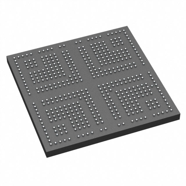
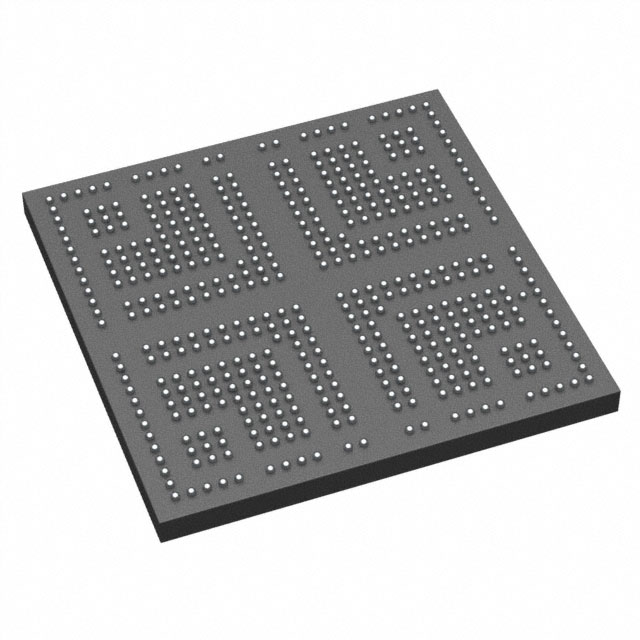
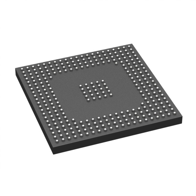
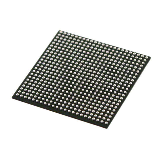
Cyclone® V GX Field Programmable Gate Array (FPGA) IC 240 7880704 149500 484-LFBGA |
|---|---|
| Quantity | 1,561 Available (as of October 7, 2026) |
| Product Category | Field Programmable Gate Array (FPGA) |
|---|---|
| Manufacturer | Intel |
| Manufacturing Status | Active |
| Manufacturer Standard Lead Time | 16 Weeks |
| Datasheet |
Specifications & Environmental
| Device Package | 484-MBGA (15x15) | Grade | Industrial | Operating Temperature | -40°C – 100°C | ||
|---|---|---|---|---|---|---|---|
| Package / Case | 484-LFBGA | Number of I/O | 240 | Voltage | 1.07 V - 1.13 V | ||
| Mounting Method | Surface Mount | RoHS Compliance | RoHS Compliant | REACH Compliance | REACH Unaffected | ||
| Moisture Sensitivity Level | 3 (168 Hours) | Number of LABs/CLBs | 56480 | Number of Logic Elements/Cells | 149500 | ||
| Number of Gates | N/A | ECCN | 3A001A2C | HTS Code | 8542.39.0001 | ||
| Qualification | N/A | Total RAM Bits | 7880704 |
Overview of 5CGXFC7B6M15I7N – Cyclone® V GX FPGA, 149,500 logic elements, 484‑LFBGA
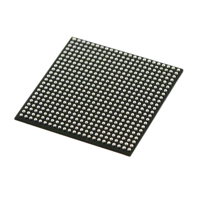
The 5CGXFC7B6M15I7N is an Intel Cyclone® V GX field‑programmable gate array (FPGA) offered in a 484‑LFBGA package. It delivers a high logic capacity of 149,500 logic elements, approximately 7.88 Mbits of embedded memory, and 240 general‑purpose I/O, making it suitable for demanding industrial and communications applications that require significant on‑chip logic and memory.
Designed for surface‑mount assembly and an industrial operating range from ‑40 °C to 100 °C, this device supports a core supply window of 1.07 V to 1.13 V and is RoHS compliant. It targets markets where integration, I/O density, and on‑chip RAM are key value drivers.
Key Features
- Logic Capacity – 149,500 logic elements to implement large combinational and sequential designs on a single FPGA.
- On‑chip Memory – Approximately 7.88 Mbits of embedded memory for frame buffers, lookup tables, and temporary data storage.
- High I/O Count – 240 user I/O pins to support multiple parallel interfaces, GPIO, and board interconnects.
- Package & Mounting – 484‑LFBGA package (supplier package listed as 484‑MBGA, 15×15) in a surface‑mount form factor for compact board layouts.
- Power – Core supply range of 1.07 V to 1.13 V to match common low‑voltage FPGA power rails.
- Industrial Temperature Grade – Rated for operation from ‑40 °C to 100 °C to meet industrial environment requirements.
- Standards & Compliance – RoHS‑compliant manufacturing and materials.
Typical Applications
- Industrial Control and Automation: Implement real‑time control, signal conditioning, and protocol bridging using the device's large logic and memory resources within industrial temperature ranges.
- Communications Infrastructure: Use the abundant logic elements and on‑chip RAM to implement packet processing, framing, and interface logic in wireless and wireline equipment.
- Defense and Test Systems: Leverage high logic density and robust temperature specifications for signal processing, data aggregation, and custom logic in military and test applications.
- High‑density I/O Systems: Deploy in multi‑port gateway, sensor aggregation, or protocol conversion designs that require 240 I/O pins for parallel connectivity.
Unique Advantages
- Substantial Logic and Memory in One Device: 149,500 logic elements combined with approximately 7.88 Mbits of embedded memory reduce the need for external logic and buffers.
- High I/O Count for Complex Interfaces: 240 I/O pins support dense board interconnects and multiple simultaneous interfaces without external multiplexing.
- Industrial‑Grade Thermal Range: Rated from ‑40 °C to 100 °C to support deployments in harsh operating environments.
- Compact, Surface‑Mount LFBGA Package: 484‑LFBGA (484‑MBGA, 15×15) packaging enables high‑density PCB layouts while maintaining manufacturing compatibility with surface‑mount processes.
- Low‑Voltage Core Operation: Narrow core supply window (1.07 V to 1.13 V) that aligns with modern low‑voltage power architectures.
- RoHS Compliance: Conforms to RoHS requirements to simplify regulatory and environmental compliance.
Why Choose 5CGXFC7B6M15I7N?
The 5CGXFC7B6M15I7N Cyclone V GX FPGA combines a large logic fabric, significant embedded memory, and a high I/O count in a single industrial‑rated, surface‑mount package. These characteristics make it well suited for applications that demand on‑chip integration of control, signal processing, and interfacing logic while operating across wide temperature ranges.
For design teams and procurement looking for scalable FPGA capacity with industrial thermal tolerance and compact packaging, this device offers a balance of integration and deployment readiness backed by Intel’s Cyclone V device family documentation and features.
Request a quote or submit an inquiry to receive pricing, availability, and additional technical information for the 5CGXFC7B6M15I7N.





















Date Founded: 1968
Headquarters: Santa Clara, California, USA
Employees: 130,000+
Revenue: $54.23 Billion
Certifications and Memberships: ISO9001:2015, ISO14001:2015, ISO17025:2017, ISO27001:2022, ISO45001:2018, ISO50001:2018


