
5SEE9F45C4N
| Part Description |
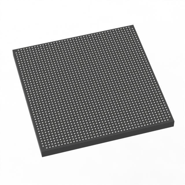
Stratix® V E Field Programmable Gate Array (FPGA) IC 840 53248000 840000 1932-BBGA, FCBGA |
|---|---|
| Quantity | 852 Available (as of June 9, 2026) |

| Product Category | Field Programmable Gate Array (FPGA) |
|---|---|
| Manufacturer | Intel |
| Manufacturing Status | Obsolete |
| Manufacturer Standard Lead Time | Contact Us |
| Datasheet |
Specifications & Environmental
| Device Package | 1932-FBGA, FC (45x45) | Grade | Commercial | Operating Temperature | 0°C – 85°C | ||
|---|---|---|---|---|---|---|---|
| Package / Case | 1932-BBGA, FCBGA | Number of I/O | 840 | Voltage | 820 mV - 880 mV | ||
| Mounting Method | Surface Mount | RoHS Compliance | RoHS Compliant | REACH Compliance | REACH Unknown | ||
| Moisture Sensitivity Level | 3 (168 Hours) | Number of LABs/CLBs | 317000 | Number of Logic Elements/Cells | 840000 | ||
| Number of Gates | N/A | ECCN | 3A001A2C | HTS Code | 8542.39.0001 | ||
| Qualification | N/A | Total RAM Bits | 53248000 |
Overview of 5SEE9F45C4N – Stratix® V E FPGA, 840,000 Logic Elements, 1932-BBGA (FCBGA)
The 5SEE9F45C4N is an Intel Stratix® V E field-programmable gate array (FPGA) in a 1932-ball BGA (FCBGA) package. It is built on a 28-nm process with an enhanced core architecture and delivers very high logic density for compute- and memory-intensive designs.
Designed for applications such as ASIC/system emulation, diagnostic imaging and instrumentation, and other data- and DSP-centric systems, this device combines a large logic fabric, abundant embedded memory, high-speed transceivers (as specified for the Stratix V family), and a dense I/O complement to support complex, bandwidth-focused designs.
Key Features
- High Logic Capacity — Approximately 840,000 logic elements to implement large FPGA designs and complex custom logic.
- Adaptive Logic Modules (ALMs) — 317,000 ALMs (adaptive logic modules) provide the building blocks for fine-grained logic synthesis and resource packing.
- Embedded Memory — Approximately 53.2 Mbits of on-chip RAM (53,248,000 bits) using M20K memory blocks for buffering, tables, and state storage.
- Variable-Precision DSP — Family-level support for variable-precision DSP blocks to accelerate multiply-accumulate and signal-processing workloads.
- Integrated Hard IP and Transceiver Technology — Stratix V family innovations include integrated hard IP blocks and low-power serial transceivers (family supports transceivers up to 28.05 Gbps) for high-bandwidth protocol implementations.
- Clocking and Fabric — Fractional PLLs and a comprehensive fabric clocking network paired with multi-track routing architecture for flexible, high-performance clocking and signal routing.
- I/O and Packaging — 840 user I/Os and a 1932-BBGA (FCBGA) package (supplier package listed as 1932-FBGA, FC 45×45) to support high-pin-count board integrations.
- Power and Temperature — Core voltage supply range of 820 mV to 880 mV; commercial operating temperature range of 0 °C to 85 °C.
- RoHS Compliant — Device is RoHS compliant for environmental compliance in applicable markets.
Typical Applications
- ASIC and System Emulation — Use the high logic density and abundant memory to prototype or emulate large ASIC designs before production.
- Diagnostic Imaging and Instrumentation — Leverage large on-chip RAM and DSP resources for real-time image processing and measurement systems.
- High-Bandwidth Networking — Implement packet processing and transport logic that benefits from dense logic fabric and the family’s high-rate transceivers.
- High-Performance DSP Systems — Deploy variable-precision DSP blocks and extensive logic to accelerate signal-processing algorithms in compute-intensive applications.
Unique Advantages
- High logic density: Approximately 840,000 logic elements enable large, feature-rich designs without partitioning across multiple devices.
- Large embedded memory: Approximately 53.2 Mbits of on-chip RAM reduces external memory dependency and simplifies board-level BOM.
- Rich DSP and timing resources: Variable-precision DSP blocks and fractional PLLs provide tailored numeric performance and flexible clocking for signal-processing chains.
- High I/O and dense packaging: 840 I/Os and a 1932-BBGA package support high-pin-count designs and intensive board-level connectivity.
- Family innovation and IP: Stratix V family features—such as integrated hard IP blocks and high-speed transceivers—help accelerate protocol implementations and reduce development risk.
- Commercial-grade operating range: Specified for 0 °C to 85 °C operation and RoHS compliance for standard commercial applications.
Why Choose 5SEE9F45C4N?
The 5SEE9F45C4N positions itself as a high-density, compute-capable Stratix V E FPGA option for teams building large-scale logic, memory-heavy, or DSP-oriented systems. Its mix of nearly one million logic elements at family level, substantial on-chip RAM, and Stratix V family transceiver and hard-IP innovations make it suitable for emulation, instrumentation, and high-bandwidth processing tasks.
For development teams seeking a commercial-grade FPGA with a clear upgrade path within the Stratix V family and the potential for low-risk transition to HardCopy ASICs, this device delivers the core architectural elements and I/O density needed to scale complex designs while leveraging the Stratix V device ecosystem and documentation.
Request a quote or submit an inquiry to obtain pricing, lead times, and availability for the 5SEE9F45C4N.


Date Founded: 1968
Headquarters: Santa Clara, California, USA
Employees: 130,000+
Revenue: $54.23 Billion
Certifications and Memberships: ISO9001:2015, ISO14001:2015, ISO17025:2017, ISO27001:2022, ISO45001:2018, ISO50001:2018


