
5SEE9F45I2L
| Part Description |
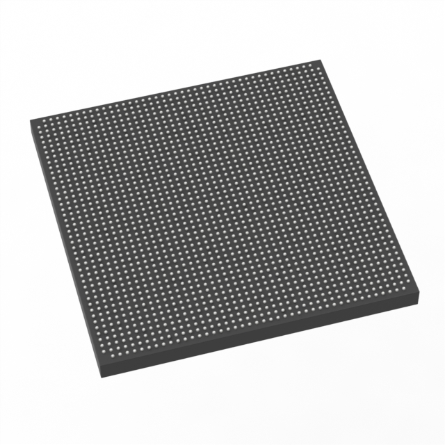
Stratix® V E Field Programmable Gate Array (FPGA) IC 840 53248000 840000 1932-BBGA, FCBGA |
|---|---|
| Quantity | 1,240 Available (as of June 15, 2026) |

| Product Category | Field Programmable Gate Array (FPGA) |
|---|---|
| Manufacturer | Intel |
| Manufacturing Status | Obsolete |
| Manufacturer Standard Lead Time | Contact Us |
| Datasheet |
Specifications & Environmental
| Device Package | 1932-FBGA, FC (45x45) | Grade | Industrial | Operating Temperature | -40°C – 100°C | ||
|---|---|---|---|---|---|---|---|
| Package / Case | 1932-BBGA, FCBGA | Number of I/O | 840 | Voltage | 820 mV - 880 mV | ||
| Mounting Method | Surface Mount | RoHS Compliance | RoHS Compliant | REACH Compliance | REACH Unknown | ||
| Moisture Sensitivity Level | 3 (168 Hours) | Number of LABs/CLBs | 317000 | Number of Logic Elements/Cells | 840000 | ||
| Number of Gates | N/A | ECCN | 3A001A2C | HTS Code | 8542.39.0001 | ||
| Qualification | N/A | Total RAM Bits | 53248000 |
Overview of 5SEE9F45I2L – Stratix® V E FPGA, 840,000 logic elements, 1932-BBGA FCBGA
The 5SEE9F45I2L is a Stratix® V E field-programmable gate array (FPGA) optimized for designs that require very high logic density and system-level integration. Built on the Stratix V family architecture, it combines an enhanced core, a large array of embedded memory and DSP resources, and integrated hard IP blocks.
Targeted applications include ASIC and system emulation, diagnostic imaging, and instrumentation; the device offers the capacity and interfaces to support data- and compute-intensive designs while operating across an industrial temperature range.
Key Features
- Core Architecture 28‑nm Stratix V family architecture with enhanced adaptive logic modules and a comprehensive fabric clocking network.
- Logic Capacity 840,000 logic elements, providing high-density programmable logic for large designs.
- Embedded Memory Approximately 53.25 Mbits of on-chip RAM (53,248,000 total RAM bits) using 20 Kbit (M20K) memory blocks as part of the device fabric.
- DSP and Hard IP Variable-precision DSP blocks and integrated hard IP options, including an Embedded HardCopy Block for hardening PCIe IP (Gen3/Gen2/Gen1) instantiations.
- I/O and Transceivers Up to 840 I/O pins and integrated high-speed transceivers (family-level support up to 28.05 Gbps), enabling broad interface and bandwidth options.
- Power Core supply voltage range of 820 mV to 880 mV to match system power requirements.
- Package and Mounting 1932‑BBGA FCBGA package (supplier device package: 1932‑FBGA, FC, 45×45); surface-mount mounting for board-level integration.
- Operating Range and Grade Industrial-grade device rated for operation from −40 °C to 100 °C and RoHS compliant.
Typical Applications
- ASIC and System Emulation High logic density makes this device suitable for prototyping and emulating large ASIC designs.
- Diagnostic Imaging Large logic and memory resources support image processing pipelines and high-throughput data handling.
- Instrumentation Integrated DSP blocks and high-speed transceivers enable advanced measurement, test, and signal-processing instruments.
- High-Bandwidth Interfaces Family-level transceiver support and hard IP blocks make the device applicable to systems requiring PCIe and other high-speed interfaces.
Unique Advantages
- High Logic Density: 840,000 logic elements provide room to integrate complex SoC-style designs without multiple devices.
- Substantial On-Chip Memory: Approximately 53.25 Mbits of embedded RAM reduces external memory dependencies and improves data locality.
- Integrated Hard IP and DSP: Embedded HardCopy capability and variable-precision DSP blocks accelerate development of compute- and protocol-intensive functions.
- Broad I/O and High-Speed Links: 840 I/O pins plus family-level transceiver support deliver flexible connectivity and bandwidth for interfacing and transport tasks.
- Industrial Temperature Range: Rated from −40 °C to 100 °C, suitable for applications requiring extended temperature operation.
- Compact, Surface-Mount Package: 1932‑BBGA FCBGA (45×45 supplier footprint) enables dense board-level integration in production systems.
Why Choose 5SEE9F45I2L?
The 5SEE9F45I2L positions itself as a high-density, industrial-grade Stratix V E FPGA that brings together a robust programmable fabric, substantial embedded memory, and integrated hard IP resources. It is suited to engineering teams and projects that need to consolidate large logic designs, accelerate DSP and protocol implementations, and support demanding data flows within a single device footprint.
With family-level features such as high-speed transceivers, Embedded HardCopy blocks, and a mature Stratix V architecture, this device offers scalability and integration potential for applications spanning emulation, imaging, instrumentation, and other compute- or bandwidth-intensive systems.
Request a quote or submit an inquiry for part number 5SEE9F45I2L to discuss availability and pricing for your project needs.


Date Founded: 1968
Headquarters: Santa Clara, California, USA
Employees: 130,000+
Revenue: $54.23 Billion
Certifications and Memberships: ISO9001:2015, ISO14001:2015, ISO17025:2017, ISO27001:2022, ISO45001:2018, ISO50001:2018


