
5SEE9F45I2LN
| Part Description |
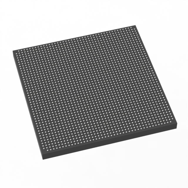
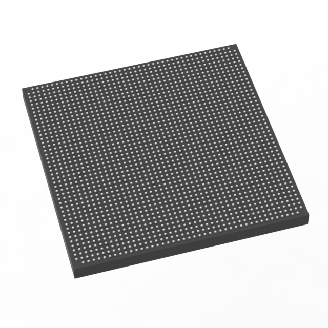
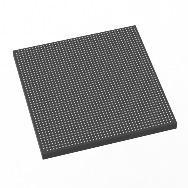
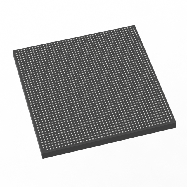
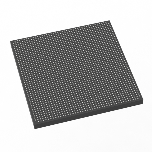
Stratix® V E Field Programmable Gate Array (FPGA) IC 840 53248000 840000 1932-BBGA, FCBGA |
|---|---|
| Quantity | 1,268 Available (as of October 7, 2026) |
| Product Category | Field Programmable Gate Array (FPGA) |
|---|---|
| Manufacturer | Intel |
| Manufacturing Status | Obsolete |
| Manufacturer Standard Lead Time | Contact Us |
| Datasheet |
Specifications & Environmental
| Device Package | 1932-FBGA, FC (45x45) | Grade | Industrial | Operating Temperature | -40°C – 100°C | ||
|---|---|---|---|---|---|---|---|
| Package / Case | 1932-BBGA, FCBGA | Number of I/O | 840 | Voltage | 820 mV - 880 mV | ||
| Mounting Method | Surface Mount | RoHS Compliance | RoHS Compliant | REACH Compliance | REACH Unknown | ||
| Moisture Sensitivity Level | 3 (168 Hours) | Number of LABs/CLBs | 317000 | Number of Logic Elements/Cells | 840000 | ||
| Number of Gates | N/A | ECCN | 3A001A2C | HTS Code | 8542.39.0001 | ||
| Qualification | N/A | Total RAM Bits | 53248000 |
Overview of 5SEE9F45I2LN – Stratix® V E FPGA, 840,000 logic elements
The 5SEE9F45I2LN is a Stratix V E field programmable gate array (FPGA) IC from Intel, built on the Stratix V family architecture. As an E-variant device it targets designs that require high logic density and large embedded memory for tasks such as ASIC/system emulation, diagnostic imaging, and instrumentation.
This device integrates approximately 840,000 logic elements and roughly 53.248 Mbits of on-chip RAM, combined with 840 I/O pins in a high-pin-count BGA package. The combination of dense logic, substantial embedded memory and broad I/O makes it suitable for complex, data- and compute-intensive FPGA implementations.
Key Features
- Core density Approximately 840,000 logic elements, delivering the logic capacity required for large-scale designs and emulation workloads.
- Embedded memory Approximately 53.248 Mbits of on-chip RAM, provided in an array of embedded memory blocks for buffering, lookup tables, and intermediate data storage.
- I/O and package 840 I/O pins in a 1932-ball BGA (FCBGA / 1932-FBGA, FC 45×45) package, supporting high-pin-count system integration and board-level routing density.
- Power supply Core voltage support in the 820 mV to 880 mV range, enabling operation within the specified low-voltage core window.
- Operating range and grade Industrial-grade device with an operating temperature range from −40 °C to 100 °C, suitable for demanding thermal environments.
- Stratix V family architecture Based on the Stratix V family building blocks noted in the datasheet — including adaptive logic modules, M20K embedded memory blocks, variable-precision DSP blocks and fractional PLLs — for flexible, high-performance implementation.
- Compliance RoHS compliant, supporting environmental and regulatory requirements for lead-free manufacturing.
Typical Applications
- ASIC and system emulation High logic density and large on-chip memory enable rapid prototyping and emulation of complex ASICs and system designs.
- Diagnostic imaging Dense logic and significant embedded RAM support the parallel processing and data buffering requirements of imaging pipelines.
- Instrumentation High I/O count and industrial temperature grade make the device suitable for laboratory and field instrumentation requiring robust signal interfacing.
- High-performance DSP applications Family-level DSP resources and memory capacity provide the building blocks needed for compute-intensive digital signal processing tasks.
Unique Advantages
- High logic capacity: Enables large, complex designs and system-level emulation without immediate external logic partitioning.
- Substantial on-chip memory: Approximately 53.248 Mbits of embedded RAM reduces dependence on external memory for many buffering and data-path tasks.
- Extensive I/O in a compact package: 840 I/Os in a 1932-ball FCBGA package support dense board-level connectivity while maintaining a manageable footprint.
- Industrial temperature rating: −40 °C to 100 °C operating range supports deployment in thermally demanding environments.
- Low-voltage core compatibility: Core supply range of 0.82 V to 0.88 V aligns with the device’s low-voltage architecture for optimized power delivery.
- Stratix V family ecosystem: Leverages documented Stratix V architecture features—such as M20K memory blocks, DSP blocks and PLLs—facilitating design reuse across the family.
Why Choose 5SEE9F45I2LN?
The 5SEE9F45I2LN positions itself as a high-density, industrial-grade Stratix V E FPGA ideal for engineers tackling complex emulation, imaging, instrumentation, and DSP challenges. With roughly 840,000 logic elements, significant embedded memory, and 840 I/Os in a 1932-ball FCBGA package, it offers the integration and capacity to simplify system design and reduce external component requirements.
Backed by the Stratix V family architecture and Intel’s documented device features, this device is suitable for development workflows that need scalable logic resources, robust I/O, and an industrial operating range—providing long-term value for projects that evolve from prototype to production.
Request a quote or submit an inquiry to specify quantities, lead times, and pricing for the 5SEE9F45I2LN. Our team can assist with ordering and technical questions to help integrate this FPGA into your design.






















Date Founded: 1968
Headquarters: Santa Clara, California, USA
Employees: 130,000+
Revenue: $54.23 Billion
Certifications and Memberships: ISO9001:2015, ISO14001:2015, ISO17025:2017, ISO27001:2022, ISO45001:2018, ISO50001:2018


