
5SGSED6K3F40I4G
| Part Description |
Stratix® V GS Field Programmable Gate Array (FPGA) IC 696 46080000 583000 1517-BBGA, FCBGA |
|---|---|
| Quantity | 759 Available (as of June 15, 2026) |

| Product Category | Field Programmable Gate Array (FPGA) |
|---|---|
| Manufacturer | Intel |
| Manufacturing Status | Active |
| Manufacturer Standard Lead Time | 26 Weeks |
| Datasheet |
Specifications & Environmental
| Device Package | 1517-FBGA (40x40) | Grade | Industrial | Operating Temperature | -40°C – 100°C | ||
|---|---|---|---|---|---|---|---|
| Package / Case | 1517-BBGA, FCBGA | Number of I/O | 696 | Voltage | 820 mV - 880 mV | ||
| Mounting Method | Surface Mount | RoHS Compliance | RoHS Compliant | REACH Compliance | REACH Unaffected | ||
| Moisture Sensitivity Level | 3 (168 Hours) | Number of LABs/CLBs | 220000 | Number of Logic Elements/Cells | 583000 | ||
| Number of Gates | N/A | ECCN | N/A | HTS Code | N/A | ||
| Qualification | N/A | Total RAM Bits | 46080000 |
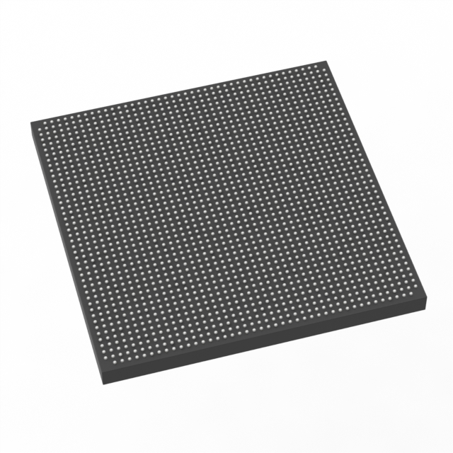
Overview of 5SGSED6K3F40I4G – Stratix® V GS FPGA, 583,000 logic elements, 696 I/O
The 5SGSED6K3F40I4G is an Intel Stratix® V GS field-programmable gate array supplied in a 1517-BBGA FCBGA package. This industrial-grade FPGA delivers large programmable logic capacity, extensive embedded memory, and a high I/O count for complex digital designs.
Designed for systems that require high-density logic, substantial on-chip RAM, and broad interface capability, this device targets applications where integration and reliability across a wide temperature range are important.
Key Features
- Core & Logic 583,000 logic elements (logic cells) and an additional 220,000 logic-related resources provide substantial programmable fabric for complex logic and datapath implementations.
- Embedded Memory Approximately 46 Mbits of total on-chip RAM to support buffering, FIFOs, and on-chip data storage requirements.
- I/O Density 696 user I/O pins to support wide parallel interfaces, multi-protocol connectivity, and dense board-level integration.
- Power Core operating voltage range specified at 820 mV to 880 mV for defined power and timing operating points.
- Package & Mounting 1517-BBGA (FCBGA) package; supplier package listed as 1517-FBGA (40×40). Device is surface-mount compatible for modern PCB assembly.
- Temperature & Grade Industrial grade operation from –40 °C to 100 °C, suitable for deployment in demanding thermal environments.
- Compliance RoHS compliant.
Typical Applications
- High-density digital processing Use the large logic capacity and embedded RAM for complex signal processing, custom compute engines, and protocol offloads.
- Communications and networking Leverage the high I/O count for multi-lane interfaces, packet processing, and high-throughput data paths.
- Industrial control and automation Industrial-temperature rating and robust I/O support motor control logic, motion systems, and factory automation controllers.
- Test, measurement and instrumentation Implement real-time data acquisition, buffering, and custom processing pipelines using on-chip memory and logic resources.
Unique Advantages
- Large programmable fabric: 583,000 logic elements enable complex designs and high gate-count implementations without external logic.
- Substantial on-chip memory: Approximately 46 Mbits of embedded RAM reduces external memory dependency and improves latency for buffering and streaming tasks.
- Extensive I/O resources: 696 I/Os accommodate multi-protocol interfacing, parallel buses, and high channel counts on a single device.
- Industrial temperature capability: Rated from –40 °C to 100 °C for reliable operation in demanding environments.
- Compact high-pin package: 1517-BBGA (1517-FBGA 40×40 supplier listing) offers a high pin count in a package suited for dense board layouts.
- Low-voltage core operation: Defined core supply window (820 mV–880 mV) supports integration with modern low-voltage power architectures.
Why Choose 5SGSED6K3F40I4G?
The 5SGSED6K3F40I4G positions itself where large-scale programmable logic, significant embedded memory, and a very high I/O count are required together with industrial temperature capability. Its combination of 583,000 logic elements, approximately 46 Mbits of on-chip RAM, and 696 I/Os makes it suitable for complex system integration tasks where consolidation of functions onto a single FPGA reduces external components and board complexity.
For design teams building advanced digital systems—communications gear, industrial controls, or data-path accelerators—this Stratix® V GS device offers a robust, verifiable specification set and packaging compatible with high-density PCBs and surface-mount assembly.
If you would like pricing, availability, or to request a formal quote for the 5SGSED6K3F40I4G, submit a quote request or product inquiry and our team will respond with the next steps.


Date Founded: 1968
Headquarters: Santa Clara, California, USA
Employees: 130,000+
Revenue: $54.23 Billion
Certifications and Memberships: ISO9001:2015, ISO14001:2015, ISO17025:2017, ISO27001:2022, ISO45001:2018, ISO50001:2018


