
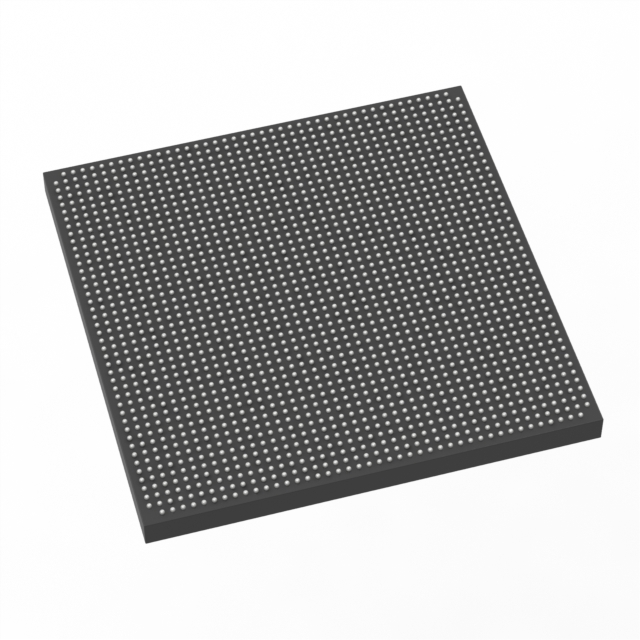
5SGSED6N1F45C2L
| Part Description |
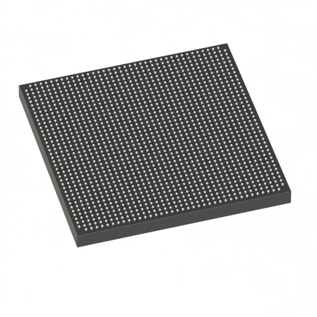
Stratix® V GS Field Programmable Gate Array (FPGA) IC 840 46080000 583000 1932-BBGA, FCBGA |
|---|---|
| Quantity | 240 Available (as of October 8, 2026) |
| Product Category | Field Programmable Gate Array (FPGA) |
|---|---|
| Manufacturer | Intel |
| Manufacturing Status | Obsolete |
| Manufacturer Standard Lead Time | Contact Us |
| Datasheet |
Specifications & Environmental
| Device Package | 1932-FBGA, FC (45x45) | Grade | Commercial | Operating Temperature | 0°C – 85°C | ||
|---|---|---|---|---|---|---|---|
| Package / Case | 1932-BBGA, FCBGA | Number of I/O | 840 | Voltage | 820 mV - 880 mV | ||
| Mounting Method | Surface Mount | RoHS Compliance | RoHS Compliant | REACH Compliance | REACH Unknown | ||
| Moisture Sensitivity Level | 3 (168 Hours) | Number of LABs/CLBs | 220000 | Number of Logic Elements/Cells | 583000 | ||
| Number of Gates | N/A | ECCN | 3A001A2C | HTS Code | 8542.39.0001 | ||
| Qualification | N/A | Total RAM Bits | 46080000 |
Overview of 5SGSED6N1F45C2L – Stratix® V GS Field Programmable Gate Array (FPGA) IC, 583,000 logic elements, 840 I/O
The 5SGSED6N1F45C2L is an Intel Stratix V GS family FPGA implemented on a 28‑nm process. It combines a high logic count with abundant DSP resources, integrated transceivers, and on‑chip embedded memory to address transceiver‑centric, DSP‑intensive designs.
Targeted use cases include transceiver‑based DSP applications and high‑bandwidth compute in markets such as wireline communications, broadcast, military, and high‑performance computing. The device’s architecture emphasizes integration and scalability for systems that require large logic capacity, extensive I/O, and significant on‑chip RAM.
Key Features
- Logic Capacity — 583,000 logic elements provide a large programmable fabric for complex ASIC‑class designs and system integration.
- Embedded Memory — Approximately 46 Mbits of on‑chip RAM implemented using 20-Kbit (M20K) memory blocks to support buffering, packet processing, and DSP data storage.
- DSP Resources — Variable‑precision DSP blocks and support for large multisplier arrays for high‑precision digital signal processing workloads; device family documentation lists specific multiplier configurations.
- Integrated Transceivers — GS‑variant transceivers with 14.1 Gbps data‑rate capability for backplane and optical interface applications.
- I/O Density — 840 I/O pins to accommodate dense system interfaces and multiport connectivity.
- Core Voltage — Low‑voltage core operation with a specified supply range of 820 mV to 880 mV for compatibility with modern low‑power system rails.
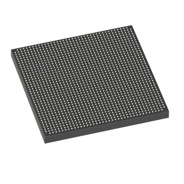
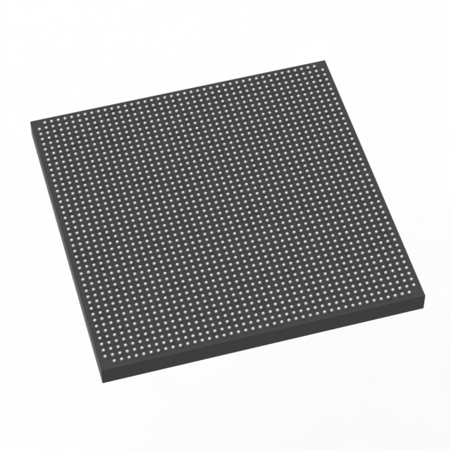
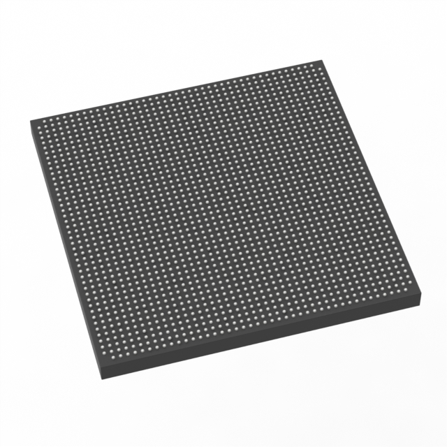
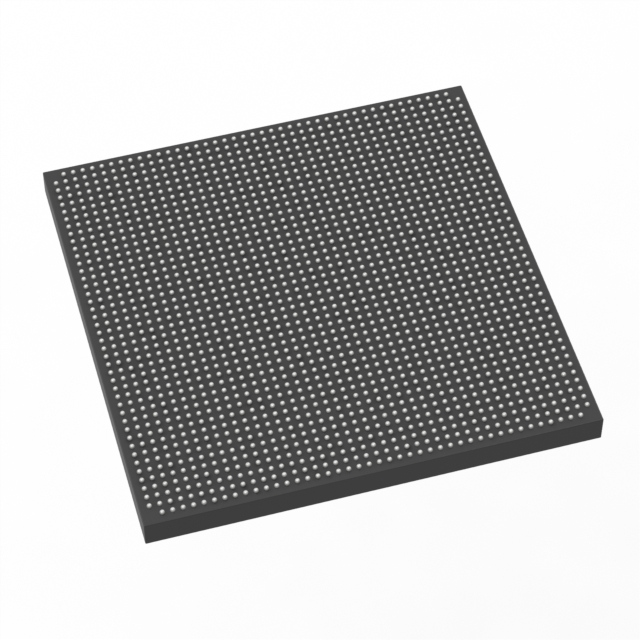
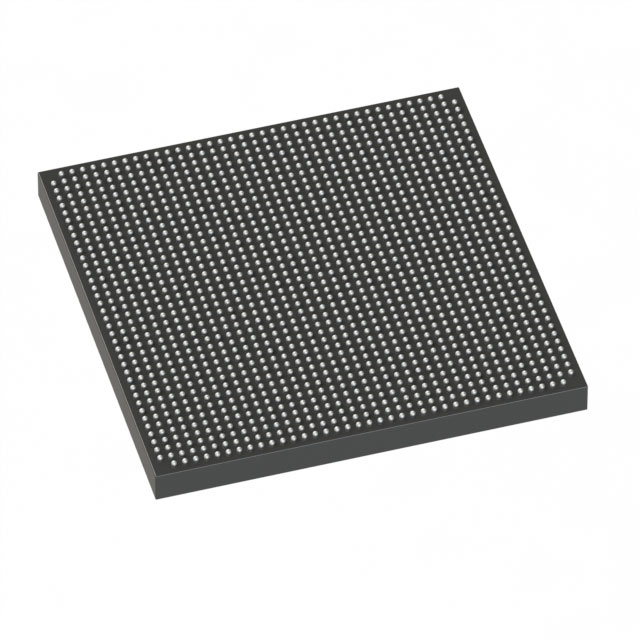
- Package — High‑density 1932‑BBGA (FCBGA) package (supplier package: 1932‑FBGA, FC 45×45) for compact board integration.
- Operating Temperature — Commercial grade operation from 0 °C to 85 °C suitable for standard electronics applications.
- Fabric Architecture — Redesigned Adaptive Logic Module (ALM), multi‑track routing architecture, and comprehensive fabric clocking network for balanced performance across logic, memory, and DSP blocks.
- Embedded HardCopy Block — On‑device Embedded HardCopy Block for hardening IP instantiations such as PCIe Gen3/Gen2/Gen1 as part of a low‑risk path toward HardCopy V ASICs.
Typical Applications
- High‑performance DSP — Algorithm acceleration and multi‑channel signal processing using variable‑precision DSP blocks and large on‑chip memory.
- Optical and Backplane Networking — Transceiver support at 14.1 Gbps and high I/O count for 40G/100G transport, switching, and packet processing subsystems.
- Broadcast and Military Communications — DSP‑centric, transceiver‑based systems that require precise signal processing and robust interface density.
- Prototyping for ASIC Migration — Use as a prototyping platform with a clear migration path to HardCopy V ASICs via the Embedded HardCopy Block.
Unique Advantages
- Substantial Logic Density: 583,000 logic elements let you consolidate complex system functions into a single device, reducing board count and BOM complexity.
- Large On‑Chip RAM: Approximately 46 Mbits of embedded memory provides local buffering and working storage for high‑throughput DSP and packet processing tasks.
- DSP‑Centric Architecture: Variable‑precision DSP blocks and multiplier support enable efficient implementation of demanding filter, encoder/decoder, and transform algorithms.
- High‑Speed I/O and Transceivers: 840 I/O and integrated 14.1 Gbps transceivers support dense, high‑bandwidth interfaces for backplane and optical links.
- Low‑Voltage Core: 820–880 mV core supply range aligns with modern low‑power system designs while maintaining performance headroom.
- ASIC Migration Path: Embedded HardCopy Block and formalized HardCopy V migration options reduce risk when moving high‑volume designs to hardened ASICs.
Why Choose 5SGSED6N1F45C2L?
The 5SGSED6N1F45C2L brings Stratix V GS architecture into systems that demand a blend of high logic capacity, extensive DSP resources, and high‑speed transceiver connectivity. Its combination of approximately 583,000 logic elements, sizable on‑chip RAM, and 14.1 Gbps transceivers makes it well suited for transceiver‑centric DSP applications and bandwidth‑intensive network processing.
This device is aimed at engineering teams building complex communications, broadcast, and computing systems that require scalable integration and a defined path to ASIC hardening. The Stratix V GS device features and architecture provide a practical balance of performance, integration, and long‑term design scalability backed by family documentation and migration options.
Request a quote or submit a purchase inquiry to get pricing and availability for the 5SGSED6N1F45C2L.





















Date Founded: 1968
Headquarters: Santa Clara, California, USA
Employees: 130,000+
Revenue: $54.23 Billion
Certifications and Memberships: ISO9001:2015, ISO14001:2015, ISO17025:2017, ISO27001:2022, ISO45001:2018, ISO50001:2018


