
5SGSED6N2F45C2
| Part Description |
Stratix® V GS Field Programmable Gate Array (FPGA) IC 840 46080000 583000 1932-BBGA, FCBGA |
|---|---|
| Quantity | 688 Available (as of June 15, 2026) |

| Product Category | Field Programmable Gate Array (FPGA) |
|---|---|
| Manufacturer | Intel |
| Manufacturing Status | Obsolete |
| Manufacturer Standard Lead Time | Contact Us |
| Datasheet |
Specifications & Environmental
| Device Package | 1932-FBGA, FC (45x45) | Grade | Commercial | Operating Temperature | 0°C – 85°C | ||
|---|---|---|---|---|---|---|---|
| Package / Case | 1932-BBGA, FCBGA | Number of I/O | 840 | Voltage | 870 mV - 930 mV | ||
| Mounting Method | Surface Mount | RoHS Compliance | RoHS non-compliant | REACH Compliance | REACH Unknown | ||
| Moisture Sensitivity Level | 3 (168 Hours) | Number of LABs/CLBs | 220000 | Number of Logic Elements/Cells | 583000 | ||
| Number of Gates | N/A | ECCN | 3A001A7A | HTS Code | 8542.39.0001 | ||
| Qualification | N/A | Total RAM Bits | 46080000 |
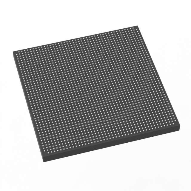
Overview of 5SGSED6N2F45C2 – Stratix® V GS FPGA, 583,000 logic elements, ~46 Mbits RAM, 840 I/Os, 1932-FBGA
The 5SGSED6N2F45C2 is a Stratix V GS field-programmable gate array (FPGA) supplied in a 1932‑FBGA surface-mount package. It implements the Stratix V family architecture on a 28‑nm process and targets transceiver-centric, DSP-heavy designs where high logic density, abundant embedded memory, and large I/O counts are required.
Typical use cases include transceiver-based DSP applications, high-bandwidth communication systems, and data‑intensive processing where a migration path to HardCopy® V ASICs can be advantageous for production. The device combines a high logic count with substantial embedded RAM and a broad I/O complement to support complex system integration.
Key Features
- Core Architecture 28‑nm Stratix V architecture delivering approximately 583,000 logic elements for dense, high-throughput logic implementations.
- Embedded Memory Approximately 46 Mbits of on-chip RAM (M20K block architecture family feature) to support large buffering, packet processing, and DSP data storage.
- Variable‑Precision DSP Resources GS‑family variable precision DSP blocks support dense multiplier configurations (family-level support for up to 3,926 18×18 or 1,963 27×27 multipliers) for high‑performance signal processing.
- High I/O Count 840 dedicated I/O pins to accommodate wide external interfaces, multi-channel transceiver routing, and complex board-level connectivity.
- Integrated Transceivers (GS family) GS devices include integrated transceivers with 14.1‑Gbps data‑rate capability for backplane and optical interface applications (Stratix V family variant feature).
- Power and Voltage Core supply range specified at 870 mV to 930 mV, enabling integration into low‑voltage FPGA power domains.
- Package and Mounting Surface‑mount 1932‑BBGA (FCBGA) footprint with a 45 × 45 mm supplier package for high‑pin‑count board designs and thermal routing.
- Commercial Grade Operating Range Rated for 0 °C to 85 °C operating temperature, suitable for standard commercial‑temperature environments.
- RoHS Compliant Conforms to RoHS environmental requirements for use in lead‑restricted assemblies.
Typical Applications
- High‑Performance DSP Systems Implement complex digital signal chains and dense multiplier arrays using the GS variable‑precision DSP blocks and abundant on‑chip RAM.
- Optical and Backplane Interfaces Leverage integrated transceivers for high‑speed serial links and packet processing in networking and telecom equipment.
- Data‑Intensive Networking Support 40G/100G and other high‑bandwidth protocols in wireline transport, switching, and packet processing applications.
- Prototyping to ASIC Migration Prototype designs on Stratix V FPGAs with a documented path to HardCopy V ASICs for production cost and performance optimization.
Unique Advantages
- High Logic Density: Approximately 583,000 logic elements enables complex SoC‑style designs and large custom logic implementations on a single device.
- Large Embedded Memory: Approximately 46 Mbits of RAM reduces reliance on external memory for buffering and temporary data storage, simplifying board design.
- DSP‑Focused Architecture: Family‑level DSP multiplier counts and variable precision support provide the arithmetic throughput required for demanding signal processing tasks.
- Extensive I/O Connectivity: 840 I/Os accommodate multi‑lane interfaces, parallel buses, and mixed-signal front ends without extensive external multiplexing.
- Production Migration Path: Stratix V devices support a low‑risk route to HardCopy V ASICs for high‑volume production runs when cost or power reduction is required.
- Commercial Temperature and RoHS Compliance: Commercial operating range and RoHS conformity ease integration into standard industry equipment and assemblies.
Why Choose 5SGSED6N2F45C2?
The 5SGSED6N2F45C2 combines the Stratix V GS device family’s DSP capabilities with a high logic count, substantial on‑chip RAM, and a large I/O set to address transceiver‑centric, compute‑intensive designs. Its 1932‑FBGA package and surface‑mount mounting support high‑density board layouts while the device’s core voltage and commercial temperature rating align with common system power and environmental requirements.
This FPGA is aimed at teams developing high‑bandwidth communications equipment, signal processing platforms, and designs that may benefit from a migration path to HardCopy V ASICs for production. The device’s feature set helps reduce external component count and simplifies integration of complex interfaces and DSP engines.
If you’d like pricing, availability, or a quote for part number 5SGSED6N2F45C2, submit a request or inquiry and our team will respond with the next steps.


Date Founded: 1968
Headquarters: Santa Clara, California, USA
Employees: 130,000+
Revenue: $54.23 Billion
Certifications and Memberships: ISO9001:2015, ISO14001:2015, ISO17025:2017, ISO27001:2022, ISO45001:2018, ISO50001:2018


