
5SGSED6N2F45C2L
| Part Description |
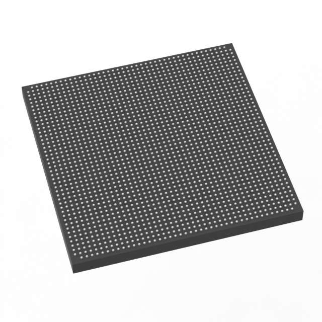
Stratix® V GS Field Programmable Gate Array (FPGA) IC 840 46080000 583000 1932-BBGA, FCBGA |
|---|---|
| Quantity | 546 Available (as of June 15, 2026) |
| Product Category | Field Programmable Gate Array (FPGA) |
|---|---|
| Manufacturer | Intel |
| Manufacturing Status | Obsolete |
| Manufacturer Standard Lead Time | Contact Us |
| Datasheet |
Specifications & Environmental
| Device Package | 1932-FBGA, FC (45x45) | Grade | Commercial | Operating Temperature | 0°C – 85°C | ||
|---|---|---|---|---|---|---|---|
| Package / Case | 1932-BBGA, FCBGA | Number of I/O | 840 | Voltage | 820 mV - 880 mV | ||
| Mounting Method | Surface Mount | RoHS Compliance | RoHS Compliant | REACH Compliance | REACH Unknown | ||
| Moisture Sensitivity Level | 3 (168 Hours) | Number of LABs/CLBs | 220000 | Number of Logic Elements/Cells | 583000 | ||
| Number of Gates | N/A | ECCN | 3A001A2C | HTS Code | 8542.39.0001 | ||
| Qualification | N/A | Total RAM Bits | 46080000 |
Overview of 5SGSED6N2F45C2L – Stratix® V GS Field Programmable Gate Array (FPGA), 583,000 Logic Elements, 1932-BBGA
The 5SGSED6N2F45C2L is a Stratix® V GS field-programmable gate array (FPGA) optimized for transceiver-driven, DSP-centric designs. Built on the Stratix V family architecture, it combines a high logic element count, abundant embedded memory, and variable-precision DSP resources to address demanding signal processing and high-bandwidth applications.
Targeted use cases include wireline communications, broadcast and military systems, and high-performance computing where on-chip DSP throughput, integrated transceivers, and large I/O capacity enable compact, high-performance implementations.
Key Features
- High logic density — Provides 583,000 logic elements to implement complex control, signal-processing, and protocol logic in a single device.
- Embedded memory — Approximately 46 Mbits of on-chip RAM (46,080,000 bits) for buffering, packet handling, and intermediate DSP storage.
- Variable-precision DSP blocks — Stratix V GS devices include variable-precision DSP resources, with family capability to support up to 3,926 18×18 or 1,963 27×27 multipliers for high-throughput arithmetic operations.
- Integrated transceiver capability — GS-family devices offer integrated transceivers with up to 14.1 Gbps data-rate capability suitable for backplane and optical interface applications.
- I/O capacity — 840 user I/O pins provide flexible interfacing to high-speed serializers/deserializers, memory, and system peripherals.
- Core architecture and routing — Stratix V family innovations include a redesigned adaptive logic module (ALM), multi-track routing architecture, and comprehensive fabric clocking to support high performance and efficient placement/routing.
- Embedded hard IP — Includes an Embedded HardCopy Block for hardened IP instantiations such as PCIe Gen1/Gen2/Gen3, supporting transitions to HardCopy ASICs when desired.
- Package and mounting — Available in a 1932-BBGA (FCBGA) package, supplier package listed as 1932-FBGA, FC (45×45); surface-mount mounting for board-level integration.
- Power and environmental — Core supply voltage range 820 mV to 880 mV; commercial operating temperature range 0 °C to 85 °C; RoHS compliant.
Typical Applications
- Wireline communications — Implements DSP-centric transceiver processing and protocol handling for backplane and transport systems.
- Broadcast and media processing — Supports high-throughput video and signal processing pipelines using dense DSP resources and on-chip memory.
- Military and aerospace systems — Enables compact, high-performance signal-processing subsystems where transceiver integration and DSP precision are required.
- High-performance computing and acceleration — Provides on-chip compute fabric and memory for algorithm acceleration and custom data-path implementations.
Unique Advantages
- Substantial on-chip resources: 583,000 logic elements and approximately 46 Mbits of embedded memory reduce reliance on external components and simplify board-level design.
- DSP-focused architecture: Variable-precision DSP blocks support dense multiply-accumulate workloads common to signal processing and algorithm acceleration.
- Transceiver-ready: GS-family transceivers with 14.1 Gbps capability enable high-speed serial links for optical and backplane interfaces.
- Hardened IP path: Embedded HardCopy Block facilitates hardened IP instantiation and supports a low-risk path to HardCopy ASICs for production scaling.
- Robust I/O footprint: 840 I/O pins provide extensive interfacing options for memory, sensors, and high-speed peripherals.
- Commercial-grade reliability: Specified for 0 °C to 85 °C operation with RoHS compliance for standard commercial deployments.
Why Choose 5SGSED6N2F45C2L?
The 5SGSED6N2F45C2L positions itself as a high-capacity, DSP-oriented Stratix V GS FPGA suited for projects that require a dense logic fabric, significant embedded memory, and integrated transceiver capability. Its combination of variable-precision DSP resources and large I/O complements designs that demand real-time signal processing and high-bandwidth interfaces.
This device is appropriate for engineers and teams building wireline, broadcast, military, and high-performance computing systems who need a scalable FPGA platform with a clear path to hardened ASIC implementations via the Stratix V family’s Embedded HardCopy capabilities.
Request a quote or submit an inquiry for 5SGSED6N2F45C2L to receive pricing and availability information for your project.


Date Founded: 1968
Headquarters: Santa Clara, California, USA
Employees: 130,000+
Revenue: $54.23 Billion
Certifications and Memberships: ISO9001:2015, ISO14001:2015, ISO17025:2017, ISO27001:2022, ISO45001:2018, ISO50001:2018


