
5SGSED6N2F45C2N
| Part Description |
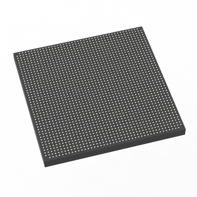
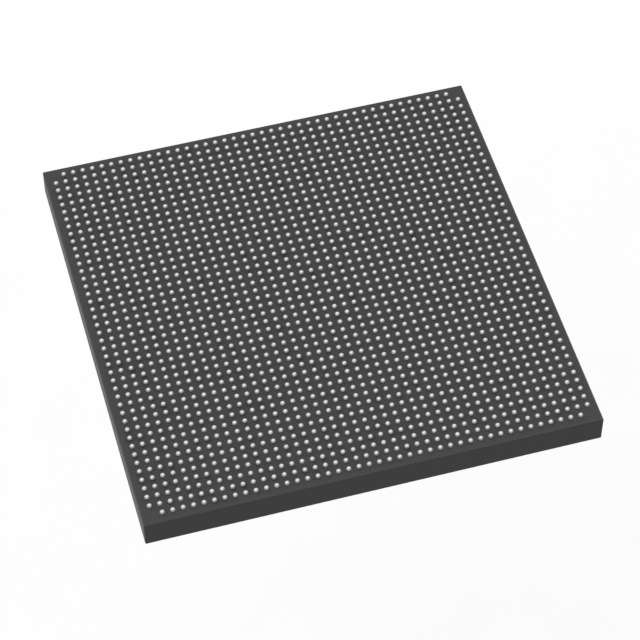
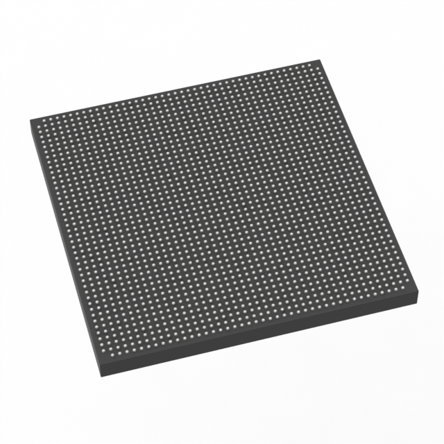
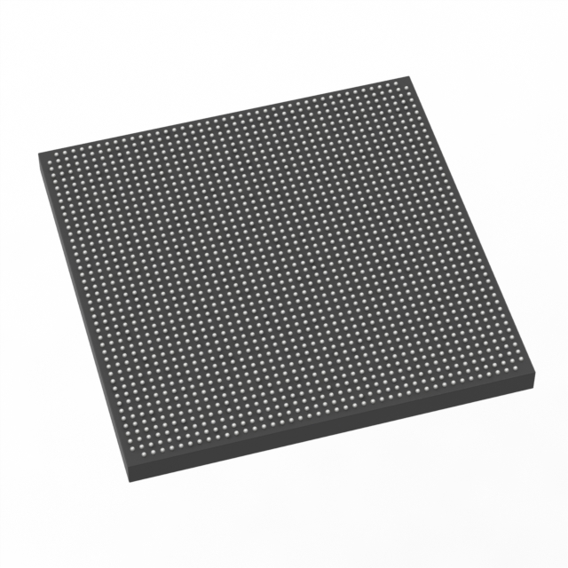
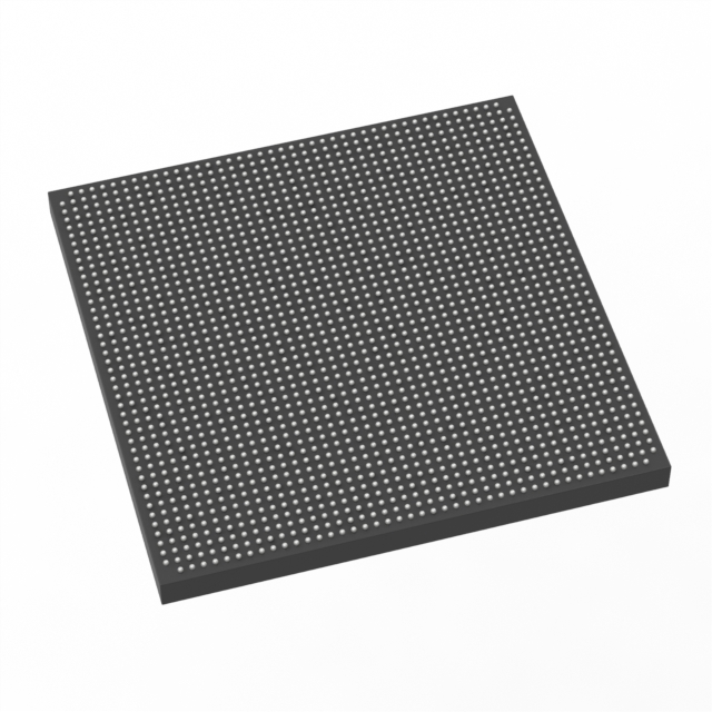
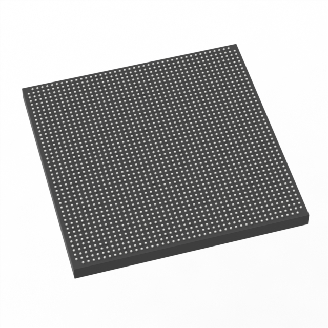
Stratix® V GS Field Programmable Gate Array (FPGA) IC 840 46080000 583000 1932-BBGA, FCBGA |
|---|---|
| Quantity | 404 Available (as of October 8, 2026) |
| Product Category | Field Programmable Gate Array (FPGA) |
|---|---|
| Manufacturer | Intel |
| Manufacturing Status | Obsolete |
| Manufacturer Standard Lead Time | Contact Us |
| Datasheet |
Specifications & Environmental
| Device Package | 1932-FBGA, FC (45x45) | Grade | Commercial | Operating Temperature | 0°C – 85°C | ||
|---|---|---|---|---|---|---|---|
| Package / Case | 1932-BBGA, FCBGA | Number of I/O | 840 | Voltage | 870 mV - 930 mV | ||
| Mounting Method | Surface Mount | RoHS Compliance | RoHS Compliant | REACH Compliance | REACH Unknown | ||
| Moisture Sensitivity Level | 3 (168 Hours) | Number of LABs/CLBs | 220000 | Number of Logic Elements/Cells | 583000 | ||
| Number of Gates | N/A | ECCN | 3A001A2C | HTS Code | 8542.39.0001 | ||
| Qualification | N/A | Total RAM Bits | 46080000 |
Overview of 5SGSED6N2F45C2N – Stratix® V GS FPGA, 583,000 logic elements, 1932-BBGA
The 5SGSED6N2F45C2N is a Stratix V GS Field Programmable Gate Array (FPGA) supplied in a 1932-BBGA (FCBGA) package. It is built on a 28-nm process and targets high-throughput, DSP-centric designs that require abundant logic, embedded memory, and on-chip transceiver support.
Engineered for commercial-grade applications, this device combines a large logic fabric and substantial embedded RAM with integrated transceiver and DSP resources to address data-intensive tasks such as packet processing, signal processing, and high-bandwidth interfaces.
Key Features
- Process & core architecture – Based on 28-nm TSMC technology with adaptive logic modules (ALMs) and a comprehensive fabric clocking network as described for the Stratix V family.
- Logic capacity – Approximately 583,000 logic elements, providing significant programmable capacity for complex FPGA designs.
- Embedded memory – Approximately 46 Mbits of on-chip RAM (total RAM bits: 46,080,000), implemented in M20K block architecture.
- DSP resources – Variable-precision DSP blocks; Stratix V GS devices support up to 3,926 18×18 or 1,963 27×27 multipliers for high-performance signal processing.
- Transceivers – Integrated transceivers with up to 14.1 Gbps data-rate capability on GS devices, suitable for backplane and optical interface applications.
- I/O density – 840 device I/Os to support wide parallel interfaces and high-density board-level connectivity.
- Package & mounting – 1932-BBGA (FCBGA) package; supplier device package listed as 1932-FBGA, FC (45×45). Surface-mount device.
- Power – Core voltage supply specified from 870 mV to 930 mV.
- Operating range – Commercial temperature grade, specified for 0 °C to 85 °C.
- System-level IP – Family-level support for Embedded HardCopy blocks, fractional PLLs, and hardened PCIe instantiation options described in Stratix V documentation.
- Environmental compliance – RoHS compliant.
Typical Applications
- High-performance DSP systems – Leverage the large pool of variable-precision DSP multipliers for applications such as broadcast processing, software-defined radio, and signal conditioning.
- Optical and backplane interfaces – Integrated transceivers with multi-gigabit capability enable backplane and optical line-card designs used in networking and telecommunications.
- Packet processing and network appliances – High logic density and abundant I/O support complex packet engines, traffic management, and protocol offload functions.
- High-bandwidth compute and test equipment – Combines large embedded memory and logic resources for data buffering, pattern generation, and high-throughput test instrumentation.
Unique Advantages
- Substantial programmable capacity: Approximately 583,000 logic elements allow large designs to be implemented without external logic expansion.
- Significant on-chip memory: Approximately 46 Mbits of embedded RAM reduces dependency on off-chip memory and improves data-path latency.
- DSP-centric architecture: Extensive variable-precision DSP multipliers provide flexibility and performance for multiply-accumulate intensive workloads.
- High I/O and transceiver integration: 840 I/Os and integrated 14.1-Gbps transceivers enable high-bandwidth interfaces and dense system integration.
- Compact, board-friendly package: 1932-BBGA/1932-FBGA (45×45) FCBGA package supports surface-mount assembly in space-constrained systems.
- Commercial thermal profile with RoHS compliance: Rated 0 °C to 85 °C and RoHS compliant for standard commercial deployments.
Why Choose 5SGSED6N2F45C2N?
The 5SGSED6N2F45C2N positions itself where high logic capacity, substantial embedded memory, and DSP/transceiver integration are required in commercial-grade systems. Its combination of approximately 583,000 logic elements, roughly 46 Mbits of on-chip RAM, and GS-class DSP/transceiver resources makes it suitable for data-intensive signal processing, network, and test applications.
Designed within the Stratix V family architecture, the device offers a known FPGA fabric and system-level hard IP capabilities that support prototyping and production deployments. For engineering teams targeting high-throughput, DSP-focused designs that require dense I/O and multi-gigabit interfaces, this FPGA provides a balanced platform of performance and integration.
Request a quote or submit a product inquiry to obtain pricing, availability, and detailed ordering information for part number 5SGSED6N2F45C2N.





















Date Founded: 1968
Headquarters: Santa Clara, California, USA
Employees: 130,000+
Revenue: $54.23 Billion
Certifications and Memberships: ISO9001:2015, ISO14001:2015, ISO17025:2017, ISO27001:2022, ISO45001:2018, ISO50001:2018


