
5SGSED6N3F45C2L
| Part Description |
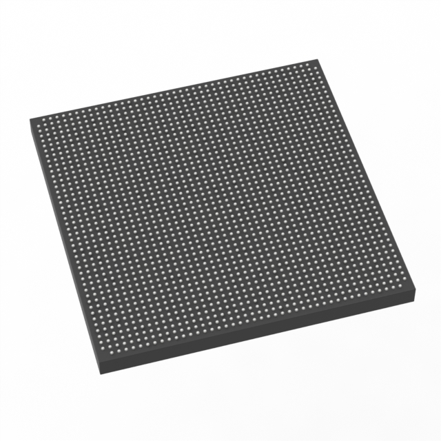
Stratix® V GS Field Programmable Gate Array (FPGA) IC 840 46080000 583000 1932-BBGA, FCBGA |
|---|---|
| Quantity | 838 Available (as of June 18, 2026) |

| Product Category | Field Programmable Gate Array (FPGA) |
|---|---|
| Manufacturer | Intel |
| Manufacturing Status | Obsolete |
| Manufacturer Standard Lead Time | Contact Us |
| Datasheet |
Specifications & Environmental
| Device Package | 1932-FBGA, FC (45x45) | Grade | Commercial | Operating Temperature | 0°C – 85°C | ||
|---|---|---|---|---|---|---|---|
| Package / Case | 1932-BBGA, FCBGA | Number of I/O | 840 | Voltage | 820 mV - 880 mV | ||
| Mounting Method | Surface Mount | RoHS Compliance | RoHS Compliant | REACH Compliance | REACH Unknown | ||
| Moisture Sensitivity Level | 3 (168 Hours) | Number of LABs/CLBs | 220000 | Number of Logic Elements/Cells | 583000 | ||
| Number of Gates | N/A | ECCN | 3A001A2C | HTS Code | 8542.39.0001 | ||
| Qualification | N/A | Total RAM Bits | 46080000 |
Overview of 5SGSED6N3F45C2L – Stratix® V GS FPGA, 583,000 logic elements
The 5SGSED6N3F45C2L is an Intel Stratix® V GS field-programmable gate array (FPGA) implemented in a 1932-ball FCBGA package. It combines a high logic-count fabric with abundant on-chip memory and DSP capability for transceiver-based, DSP-centric and data-intensive designs.
Built on the Stratix V device family architecture, this GS variant targets applications that require large FPGA logic resources, substantial embedded memory, and high I/O density while operating within a commercial temperature range.
Key Features
- Logic Capacity — 583,000 logic elements provide substantial programmable fabric for complex algorithms and system integration.
- Embedded Memory — Approximately 46 Mbits of on-chip RAM (46,080,000 total RAM bits) to support buffers, lookup tables, and packet or signal processing data storage.
- DSP Resources (Stratix V GS) — Stratix V GS devices include variable-precision DSP blocks; the family supports large numbers of multipliers for high-precision DSP implementations.
- I/O Density — 840 I/Os enable dense board-level connectivity for multi-channel interfaces, high-speed links, and control paths.
- Transceiver and Hard IP (family) — Stratix V family devices feature integrated transceivers and hard IP blocks; the family provides transceiver options up to 28.05 Gbps and Embedded HardCopy Blocks for hardened PCIe IP instantiation.
- Power and Supply — Core supply voltage range from 820 mV to 880 mV for the device core.
- Package — 1932-BBGA, FCBGA package; supplier device package listed as 1932-FBGA FC (45×45) for compact, surface-mount assembly.
- Operating Range — Commercial grade operation from 0 °C to 85 °C.
- Compliance — RoHS compliant.
Typical Applications
- High-performance DSP systems — Leverage abundant DSP blocks and large logic capacity for filtering, transform engines, and real-time signal processing.
- Data-center and networking equipment — Use the device’s high logic count, embedded memory, and transceiver-capable family architecture for packet processing and protocol offload in 40G/100G-class systems.
- Broadcast and wireline communications — Implement channel processing, multiplexing, and high-throughput transport functions with the device’s I/O and memory resources.
- Prototyping for ASIC migration — Stratix V FPGAs support low-risk prototyping paths toward HardCopy V ASIC conversions through embedded hard IP blocks.
Unique Advantages
- High programmable capacity: 583,000 logic elements enable integration of complex system functions into a single device, reducing board-level component count.
- Substantial on-chip RAM: Approximately 46 Mbits of embedded memory supports large buffering and state storage without relying on external memory for many use cases.
- Dense I/O footprint: 840 I/Os provide flexibility for multi-protocol interfaces, channel-rich designs, and broad system connectivity.
- Family-level transceiver and hard IP support: Stratix V family innovations include high-speed transceivers and Embedded HardCopy Blocks for hardened PCIe implementations, simplifying high-speed interface integration.
- Commercial-grade deployment: Specified for 0 °C to 85 °C operation and RoHS compliance for standard commercial applications.
- Compact, surface-mount package: 1932-ball FCBGA (45×45) packaging balances high pin count and board-area efficiency for dense system designs.
Why Choose 5SGSED6N3F45C2L?
The 5SGSED6N3F45C2L positions itself for designs that demand extensive programmable logic, sizable on-chip memory, and a high number of I/Os within a commercial temperature range. As a Stratix V GS device, it aligns with transceiver-based, DSP-centric and data-intensive applications where integration and throughput are priorities.
Choosing this FPGA gives teams a scalable prototyping platform within the Stratix V family, with on-device resources and family-level hard IP to accelerate development and support potential migration paths to hardened ASIC implementations.
Request a quote or submit a pricing and availability inquiry to move your design forward with the 5SGSED6N3F45C2L Stratix V GS FPGA.


Date Founded: 1968
Headquarters: Santa Clara, California, USA
Employees: 130,000+
Revenue: $54.23 Billion
Certifications and Memberships: ISO9001:2015, ISO14001:2015, ISO17025:2017, ISO27001:2022, ISO45001:2018, ISO50001:2018


