
5SGSED6N3F45C2N
| Part Description |
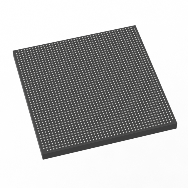
Stratix® V GS Field Programmable Gate Array (FPGA) IC 840 46080000 583000 1932-BBGA, FCBGA |
|---|---|
| Quantity | 1,406 Available (as of June 15, 2026) |

| Product Category | Field Programmable Gate Array (FPGA) |
|---|---|
| Manufacturer | Intel |
| Manufacturing Status | Obsolete |
| Manufacturer Standard Lead Time | Contact Us |
| Datasheet |
Specifications & Environmental
| Device Package | 1932-FBGA, FC (45x45) | Grade | Commercial | Operating Temperature | 0°C – 85°C | ||
|---|---|---|---|---|---|---|---|
| Package / Case | 1932-BBGA, FCBGA | Number of I/O | 840 | Voltage | 870 mV - 930 mV | ||
| Mounting Method | Surface Mount | RoHS Compliance | RoHS Compliant | REACH Compliance | REACH Unknown | ||
| Moisture Sensitivity Level | 3 (168 Hours) | Number of LABs/CLBs | 220000 | Number of Logic Elements/Cells | 583000 | ||
| Number of Gates | N/A | ECCN | 3A001A2C | HTS Code | 8542.39.0001 | ||
| Qualification | N/A | Total RAM Bits | 46080000 |
Overview of 5SGSED6N3F45C2N – Stratix® V GS FPGA, 840 I/O, 583,000 logic elements
The 5SGSED6N3F45C2N is a Stratix V GS field‑programmable gate array supplied in a 1932‑FBGA (45×45 mm) surface‑mount package. It delivers high logic capacity and on‑chip memory along with the transceiver and DSP‑centric features characteristic of the Stratix V GS family.
Targeted at bandwidth‑ and DSP‑intensive designs, this commercial‑grade device is suited for applications that require large logic fabric, abundant embedded memory, extensive I/O, and family‑level transceiver and DSP capabilities.
Key Features
- Logic Capacity — 583,000 logic elements for implementing large, complex digital designs.
- Embedded Memory — Approximately 46 Mbits of on‑chip RAM to support buffering and data‑intensive functions.
- DSP‑Oriented Family Features — As part of the Stratix V GS family, the device benefits from variable‑precision DSP blocks and family support for up to 3,926 18×18 or 1,963 27×27 multipliers (family-level specification).
- Integrated Transceivers (family‑level) — Stratix V GS devices provide integrated transceivers with up to 14.1 Gbps data‑rate capability (family-level specification).
- I/O Density — 840 user I/O pins to interface with high‑pin‑count systems and dense connector requirements.
- Power — Core supply range of 870 mV to 930 mV to match system power design constraints.
- Package and Mounting — 1932‑BBGA (FCBGA) package, supplier package 1932‑FBGA, FC (45×45), surface‑mount for standard PCB assembly flows.
- Operating Range & Grade — Commercial grade operation from 0 °C to 85 °C.
- Environmental Compliance — RoHS compliant.
Typical Applications
- High‑performance DSP systems — Leverages Stratix V GS family DSP resources for filtering, transforms, and precision signal processing workloads.
- High‑bandwidth communications — Supports transceiver‑centric implementations for backplane, optical interface, and packet processing where multi‑Gbps links are required (family‑level transceiver capability).
- Network and telecom equipment — Large logic capacity, abundant embedded RAM, and high I/O count enable complex protocol processing and buffering for 40G/100G systems (as targeted by the Stratix V family).
- High‑performance computing and broadcast — Combines logic density and DSP resources for compute‑intensive signal paths and format conversions common in HPC and broadcast applications.
Unique Advantages
- High logic capacity: 583,000 logic elements accommodate large digital designs without immediate partitioning across multiple devices.
- Substantial on‑chip memory: Approximately 46 Mbits of embedded RAM reduces external memory dependence for buffering and temporary storage.
- Extensive I/O: 840 user I/O pins support high‑density interfaces and multiple simultaneous high‑speed signals.
- DSP and transceiver family pedigree: As a Stratix V GS device, it aligns with family features for variable‑precision DSP blocks and integrated transceivers (family‑level specs) for DSP‑centric, transceiver‑based designs.
- Compact surface‑mount package: 1932‑FBGA (45×45 mm) provides high pin count in a single‑device footprint for compact system layouts.
- Commercial operating range and RoHS compliance: Designed for 0 °C to 85 °C operation and manufactured to meet RoHS requirements.
Why Choose 5SGSED6N3F45C2N?
The 5SGSED6N3F45C2N places the Stratix V GS family’s DSP and transceiver strengths into a single, high‑capacity FPGA package. With 583,000 logic elements, approximately 46 Mbits of embedded RAM, and 840 I/O, it is positioned for designers building data‑intensive and signal‑processing systems that require substantial on‑chip resources and dense interfaces.
As part of the Stratix V family, this device benefits from the documented family‑level architecture and resources, offering a clear development path for bandwidth‑ and DSP‑centric applications while fitting standard surface‑mount assembly and commercial operating environments.
Request a quote or submit a product inquiry to get pricing and availability information for the 5SGSED6N3F45C2N.


Date Founded: 1968
Headquarters: Santa Clara, California, USA
Employees: 130,000+
Revenue: $54.23 Billion
Certifications and Memberships: ISO9001:2015, ISO14001:2015, ISO17025:2017, ISO27001:2022, ISO45001:2018, ISO50001:2018


