
5SGSED6N3F45I3G
| Part Description |
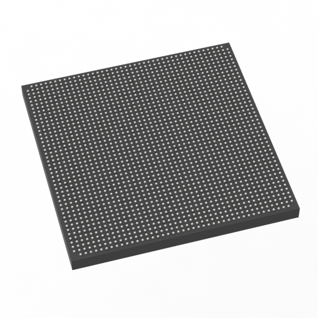
Stratix® V GS Field Programmable Gate Array (FPGA) IC 840 46080000 583000 1932-BBGA, FCBGA |
|---|---|
| Quantity | 1,091 Available (as of June 10, 2026) |

| Product Category | Field Programmable Gate Array (FPGA) |
|---|---|
| Manufacturer | Intel |
| Manufacturing Status | Active |
| Manufacturer Standard Lead Time | 26 Weeks |
| Datasheet |
Specifications & Environmental
| Device Package | 1932-FBGA, FC (45x45) | Grade | Industrial | Operating Temperature | -40°C – 100°C | ||
|---|---|---|---|---|---|---|---|
| Package / Case | 1932-BBGA, FCBGA | Number of I/O | 840 | Voltage | 820 mV - 880 mV | ||
| Mounting Method | Surface Mount | RoHS Compliance | RoHS Compliant | REACH Compliance | REACH Unaffected | ||
| Moisture Sensitivity Level | 3 (168 Hours) | Number of LABs/CLBs | 220000 | Number of Logic Elements/Cells | 583000 | ||
| Number of Gates | N/A | ECCN | N/A | HTS Code | N/A | ||
| Qualification | N/A | Total RAM Bits | 46080000 |
Overview of 5SGSED6N3F45I3G – Stratix® V GS FPGA IC, 583,000 logic elements
The 5SGSED6N3F45I3G is a Stratix® V GS field programmable gate array (FPGA) in a 1932-BBGA FCBGA package, manufactured by Intel. This industrial-grade FPGA provides very large logic capacity, substantial on-chip memory, and a high I/O count suitable for complex, high-density digital designs.
Designed for applications that require extensive programmable logic, abundant embedded memory, and wide connectivity, the device targets system designs where integration, thermal range, and board-level packaging are key considerations.
Key Features
- Logic Capacity 583,000 logic elements enabling high-density programmable logic implementations.
- Embedded Memory Approximately 46 Mbits of on-chip RAM (46,080,000 total RAM bits) to support memory-intensive algorithms and buffering.
- High I/O Count 840 I/O pins to accommodate large numbers of external interfaces and parallel connections.
- Core Voltage Operates at a core supply range of 820–880 mV, supporting low-voltage core operation requirements.
- Package & Mounting 1932-BBGA FCBGA package (supplier package: 1932-FBGA, FC 45×45) with surface-mount mounting for compact board-level integration.
- Temperature & Grade Industrial grade device rated for operation from –40 °C to 100 °C, suitable for extended-temperature applications.
- RoHS Compliant Device meets RoHS requirements for restricted substances.
Typical Applications
- High-density digital processing Large-scale logic implementations that leverage 583,000 logic elements for complex state machines, custom accelerators, and parallel datapaths.
- Memory-intensive algorithms Designs requiring substantial on-chip buffering and working memory can use the device’s approximately 46 Mbits of embedded RAM.
- High-connectivity systems Systems that need many external interfaces—sensors, buses, or parallel I/O—can take advantage of the 840 I/O pins.
- Industrial controls and equipment Applications demanding an industrial temperature range (–40 °C to 100 °C) and durable packaging for long-term deployment.
Unique Advantages
- High logic density: 583,000 logic elements provide the capacity to consolidate multiple functions into a single FPGA, reducing board-level component count.
- Significant on-chip memory: Approximately 46 Mbits of RAM enables local data storage for buffering, lookup tables, and streaming algorithms without external memory dependencies.
- Extensive I/O availability: 840 I/O pins simplify integration with large sensor arrays, parallel interfaces, or multi-channel data paths.
- Industrial temperature rating: Operation from –40 °C to 100 °C supports deployments in harsher environments where extended temperature performance is required.
- Compact FCBGA packaging: The 1932-ball FCBGA (45×45) surface-mount package enables high pin density in a compact footprint for space-constrained PCBs.
- Low-voltage core operation: Core supply range of 820–880 mV supports designs optimized for low-voltage power domains.
Why Choose 5SGSED6N3F45I3G?
The 5SGSED6N3F45I3G positions itself as a high-capacity, industrial-grade Stratix V GS FPGA that balances large programmable logic resources, substantial embedded memory, and a high I/O count in a single FCBGA package. Its core voltage range and surface-mount 1932-ball package make it suitable for compact, power-conscious systems that still require significant on-chip resources.
This device is well suited to engineering teams building complex digital systems that need scalability and robust thermal performance. Backed by the Stratix V device documentation, the part is intended for designs where integration density, on-chip memory, and broad connectivity are primary requirements.
Request a quote or submit an inquiry to receive pricing and availability information for the 5SGSED6N3F45I3G Stratix® V GS FPGA.


Date Founded: 1968
Headquarters: Santa Clara, California, USA
Employees: 130,000+
Revenue: $54.23 Billion
Certifications and Memberships: ISO9001:2015, ISO14001:2015, ISO17025:2017, ISO27001:2022, ISO45001:2018, ISO50001:2018


