
5SGSMD3H1F35C2L
| Part Description |
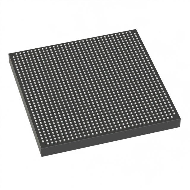
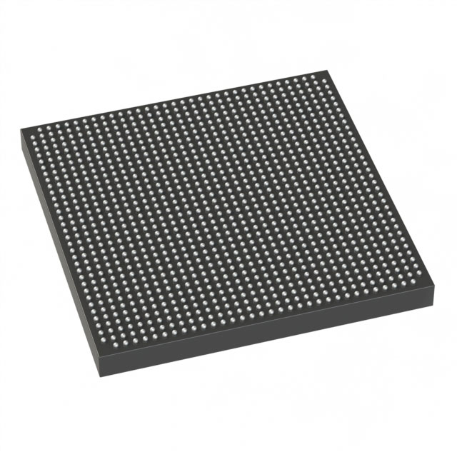
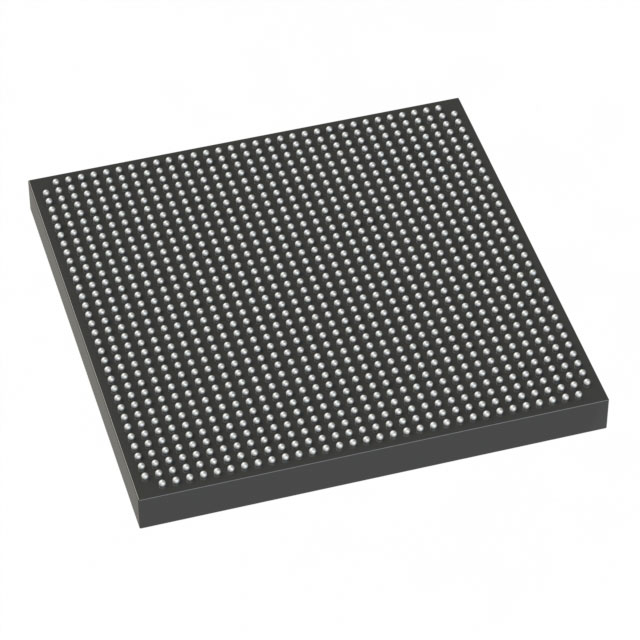
Stratix® V GS Field Programmable Gate Array (FPGA) IC 432 13312000 236000 1152-BBGA, FCBGA |
|---|---|
| Quantity | 224 Available (as of October 8, 2026) |
| Product Category | Field Programmable Gate Array (FPGA) |
|---|---|
| Manufacturer | Intel |
| Manufacturing Status | Obsolete |
| Manufacturer Standard Lead Time | Contact Us |
| Datasheet |
Specifications & Environmental
| Device Package | 1152-FBGA (35x35) | Grade | Commercial | Operating Temperature | 0°C – 85°C | ||
|---|---|---|---|---|---|---|---|
| Package / Case | 1152-BBGA, FCBGA | Number of I/O | 432 | Voltage | 820 mV - 880 mV | ||
| Mounting Method | Surface Mount | RoHS Compliance | RoHS Compliant | REACH Compliance | REACH Unknown | ||
| Moisture Sensitivity Level | 3 (168 Hours) | Number of LABs/CLBs | 89000 | Number of Logic Elements/Cells | 236000 | ||
| Number of Gates | N/A | ECCN | 3A001A2C | HTS Code | 8542.39.0001 | ||
| Qualification | N/A | Total RAM Bits | 13312000 |
Overview of 5SGSMD3H1F35C2L – Stratix V GS FPGA, 1152‑FBGA (35×35)
The 5SGSMD3H1F35C2L is an Intel Stratix® V GS field‑programmable gate array supplied in a 1152‑FBGA (35×35) surface‑mount package. Built on the Stratix V family architecture, this GS variant targets DSP‑centric, transceiver‑enabled designs where high logic density and substantial on‑chip memory are required.
With 236,000 logic elements, approximately 13.3 Mbits of embedded RAM, 432 I/Os, and a core supply range of 820 mV to 880 mV, this device is suited for bandwidth and compute‑intensive applications that operate in commercial temperature environments (0 °C to 85 °C).
Key Features
- Stratix V architecture Enhanced core architecture from the Stratix V family, delivering the building blocks used across GS devices.
- Logic density 236,000 logic elements to implement complex combinational and sequential logic.
- Embedded memory Approximately 13.3 Mbits of on‑chip RAM for buffering, packet processing, and intermediate storage.
- DSP and multiplier resources GS family devices include abundant variable‑precision DSP blocks; the family supports up to 3,926 18×18 or 1,963 27×27 multipliers (family specification).
- High‑speed transceivers (family) Stratix V GS devices provide integrated transceivers with 14.1‑Gbps data‑rate capability (family specification) for backplane and optical interfaces.
- Embedded HardCopy block (family) The family includes an Embedded HardCopy Block that can harden IP instantiations such as PCIe Gen3/Gen2/Gen1 (family specification).
- I/O and package 432 user I/Os in a 1152‑BBGA/FCBGA surface‑mount package (1152‑FBGA, 35×35 mm supplier package).
- Power and thermal Core voltage supply range 820 mV to 880 mV; rated for commercial operation from 0 °C to 85 °C.
- Compliance RoHS‑compliant material status.
Typical Applications
- High‑performance DSP systems Use the GS device’s variable‑precision DSP blocks and large logic fabric for signal processing, filtering, and acceleration tasks.
- Packet processing and networking Leverage the large on‑chip memory and 432 I/Os for buffering, packet lookup, and interface aggregation in network equipment.
- Optical and backplane interfaces The family’s 14.1‑Gbps transceiver capability supports high‑speed serial links for optical transport and backplane connectivity.
- Prototyping for ASIC migration Use the Stratix V family device and Embedded HardCopy block approach to prototype designs intended for HardCopy conversions.
Unique Advantages
- Substantial logic capacity: 236,000 logic elements enable integration of complex control, datapath, and protocol logic within a single device, reducing board‑level part count.
- Significant on‑chip RAM: Approximately 13.3 Mbits of embedded memory supports large buffering and table storage without external memory dependencies.
- Transceiver and DSP balance (family): The GS family combines transceiver capability with abundant DSP resources, making it well suited for transceiver‑based signal processing workloads.
- Commercial temperature rating: Specification for 0 °C to 85 °C operation aligns with standard commercial product environments and system integration requirements.
- Compact, surface‑mount package: 1152‑FBGA (35×35) package provides high I/O density in a compact footprint for space‑constrained designs.
- RoHS compliance: Meets RoHS requirements for lead‑free manufacturing and deployment.
Why Choose 5SGSMD3H1F35C2L?
The 5SGSMD3H1F35C2L delivers a combination of high logic density, substantial embedded memory, and a large I/O complement in a commercial‑grade Stratix V GS device. It is positioned for designs that require DSP horsepower alongside high‑speed serial capability and on‑chip storage, while remaining within standard commercial thermal and supply constraints.
This device is suitable for engineering teams developing bandwidth‑centric and data‑intensive systems who need a proven Stratix V family architecture with the option to leverage family features such as variable‑precision DSP blocks and Embedded HardCopy hardening for production migration.
Request a quote or submit an inquiry to obtain pricing and availability for 5SGSMD3H1F35C2L. Provide part number and required quantity when requesting a quote.





















Date Founded: 1968
Headquarters: Santa Clara, California, USA
Employees: 130,000+
Revenue: $54.23 Billion
Certifications and Memberships: ISO9001:2015, ISO14001:2015, ISO17025:2017, ISO27001:2022, ISO45001:2018, ISO50001:2018


