
5SGSMD3H1F35C2N
| Part Description |
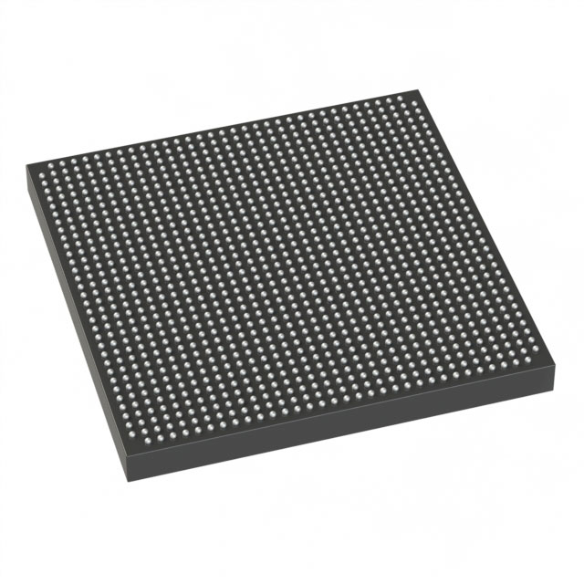
Stratix® V GS Field Programmable Gate Array (FPGA) IC 432 13312000 236000 1152-BBGA, FCBGA |
|---|---|
| Quantity | 1,047 Available (as of June 10, 2026) |

| Product Category | Field Programmable Gate Array (FPGA) |
|---|---|
| Manufacturer | Intel |
| Manufacturing Status | Obsolete |
| Manufacturer Standard Lead Time | Contact Us |
| Datasheet |
Specifications & Environmental
| Device Package | 1152-FBGA (35x35) | Grade | Commercial | Operating Temperature | 0°C – 85°C | ||
|---|---|---|---|---|---|---|---|
| Package / Case | 1152-BBGA, FCBGA | Number of I/O | 432 | Voltage | 870 mV - 930 mV | ||
| Mounting Method | Surface Mount | RoHS Compliance | RoHS Compliant | REACH Compliance | REACH Unknown | ||
| Moisture Sensitivity Level | 3 (168 Hours) | Number of LABs/CLBs | 89000 | Number of Logic Elements/Cells | 236000 | ||
| Number of Gates | N/A | ECCN | 3A001A2C | HTS Code | 8542.39.0001 | ||
| Qualification | N/A | Total RAM Bits | 13312000 |
Overview of 5SGSMD3H1F35C2N – Stratix® V GS FPGA, 1152-BBGA FCBGA (35×35)
The 5SGSMD3H1F35C2N is a Stratix V GS field-programmable gate array (FPGA) optimized for DSP-centric and transceiver-based applications. Built on the Stratix V family architecture, it combines large logic capacity with abundant on-chip memory and high-speed I/O to address bandwidth- and compute-intensive designs.
This device targets markets that require high precision digital signal processing, backplane and optical interfaces, and data throughput, offering a balance of performance, integration, and commercial-grade operation.
Key Features
- Logic Capacity — 236,000 logic elements to implement complex programmable logic and custom processing pipelines.
- Embedded Memory — Approximately 13.3 Mbits of on-chip RAM (13,312,000 bits) for buffering, FIFOs, and large on-die data structures.
- DSP Resources — Stratix V GS family devices include variable-precision DSP blocks; GS devices support up to 3,926 18×18 or 1,963 27×27 multipliers for high-performance DSP algorithms.
- High-speed Transceivers — GS variant includes integrated transceivers with 14.1‑Gbps data-rate capability for backplane and optical interface applications.
- I/O Density — 432 I/O pins to support broad peripheral and interface connectivity requirements.
- Process and Core Voltage — 28-nm TSMC process technology with device core voltages around 0.85 V or 0.9 V; this part’s documented supply range is 870 mV to 930 mV.
- Package & Mounting — 1152-ball BBGA, FCBGA footprint; supplier package listed as 1152-FBGA (35×35). Surface-mount mounting type.
- Operating Conditions — Commercial grade with an operating temperature range of 0 °C to 85 °C and RoHS compliance.
Typical Applications
- High-performance DSP systems — Use the abundant DSP blocks and large on-chip RAM to implement multi-channel filters, FFTs, and precision signal-processing pipelines.
- Optical and Backplane Interfaces — Integrated 14.1‑Gbps transceivers enable implementation of 40G/100G interfaces and high-speed serial links for packet processing and transport equipment.
- Network and Telecom Equipment — High logic density and I/O count support complex packet processing, traffic management, and protocol offload functions.
- Compute Acceleration — Combine logic elements, DSP multipliers, and embedded memory for application-specific acceleration in broadcast, test, and communications systems.
Unique Advantages
- Large, programmable fabric: 236,000 logic elements enable integration of substantial custom logic and state machines within a single device, reducing board-level complexity.
- Significant on-chip memory: Approximately 13.3 Mbits of embedded RAM provide local storage for buffering and latency-sensitive data, minimizing external memory dependence.
- Dedicated DSP capability: GS family DSP resources (supporting thousands of multipliers) accelerate multiply-accumulate workloads common in signal processing and compute tasks.
- High-speed serial I/O: Integrated transceivers with 14.1‑Gbps capability simplify implementation of high-bandwidth links for optical and backplane systems.
- Commercial-grade thermal and power: Documented operating range (0 °C to 85 °C) and a defined core supply range (870 mV–930 mV) support predictable system integration and power budgeting.
- RoHS compliant: Meets RoHS environmental requirements for streamlined regulatory compliance in standard commercial products.
Why Choose 5SGSMD3H1F35C2N?
This Stratix V GS device positions itself for designers who need a high-capacity, DSP-optimized FPGA with integrated high-speed serial I/O and substantial embedded memory. Its combination of logic density, DSP resources, and transceiver capability makes it well suited for communications, broadcast, test, and compute-acceleration designs where on-chip performance and integration reduce system complexity.
For teams building bandwidth- and compute-intensive systems, the 5SGSMD3H1F35C2N provides a commercially graded, RoHS-compliant solution that maps complex algorithms and high-speed interfaces into a single 1152-ball FCBGA package.
If you need pricing or availability for 5SGSMD3H1F35C2N, request a quote or submit an inquiry for expedited handling and supply information.


Date Founded: 1968
Headquarters: Santa Clara, California, USA
Employees: 130,000+
Revenue: $54.23 Billion
Certifications and Memberships: ISO9001:2015, ISO14001:2015, ISO17025:2017, ISO27001:2022, ISO45001:2018, ISO50001:2018


