
5SGSMD3H1F35I2G
| Part Description |
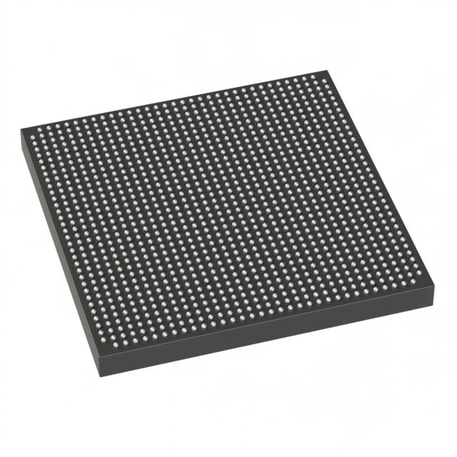
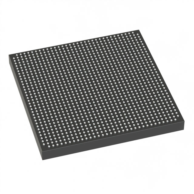
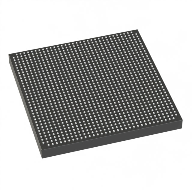
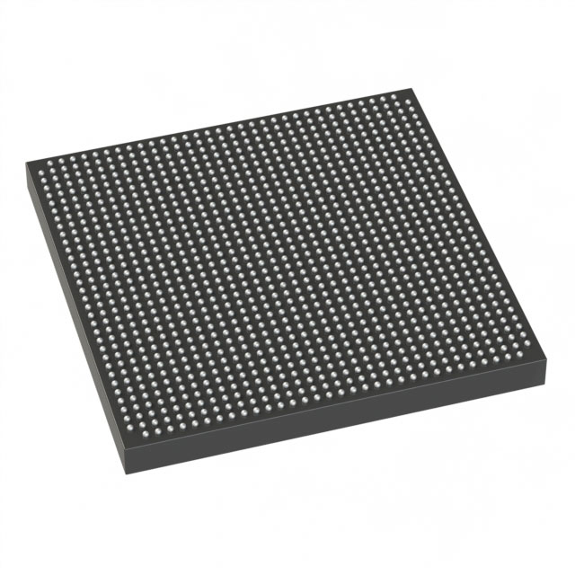
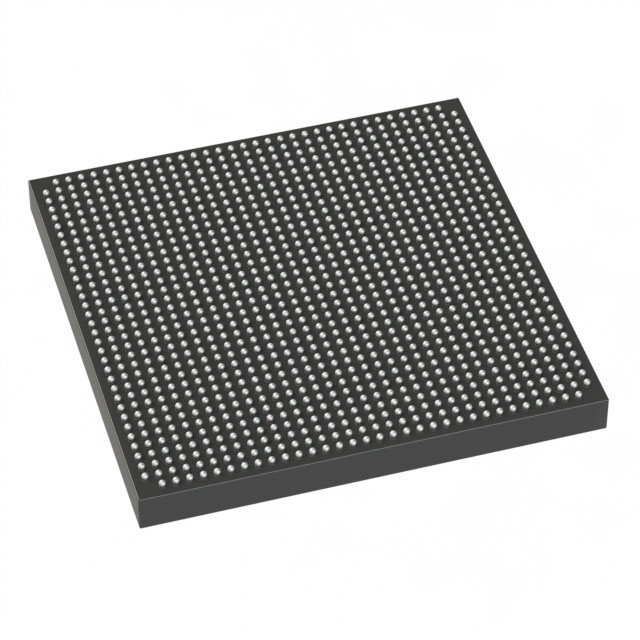
Stratix® V GS Field Programmable Gate Array (FPGA) IC 432 13312000 236000 1152-BBGA, FCBGA |
|---|---|
| Quantity | 197 Available (as of October 7, 2026) |
| Product Category | Field Programmable Gate Array (FPGA) |
|---|---|
| Manufacturer | Intel |
| Manufacturing Status | Active |
| Manufacturer Standard Lead Time | 26 Weeks |
| Datasheet |
Specifications & Environmental
| Device Package | 1152-FBGA (35x35) | Grade | Industrial | Operating Temperature | -40°C – 100°C | ||
|---|---|---|---|---|---|---|---|
| Package / Case | 1152-BBGA, FCBGA | Number of I/O | 432 | Voltage | 870 mV - 930 mV | ||
| Mounting Method | Surface Mount | RoHS Compliance | RoHS Compliant | REACH Compliance | REACH Unaffected | ||
| Moisture Sensitivity Level | 3 (168 Hours) | Number of LABs/CLBs | 89000 | Number of Logic Elements/Cells | 236000 | ||
| Number of Gates | N/A | ECCN | N/A | HTS Code | N/A | ||
| Qualification | N/A | Total RAM Bits | 13312000 |
Overview of 5SGSMD3H1F35I2G – Stratix® V GS Field Programmable Gate Array (FPGA), 432 I/Os, 236,000 logic elements, 1152-BBGA
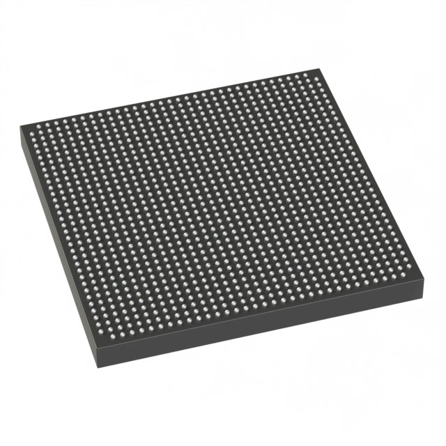
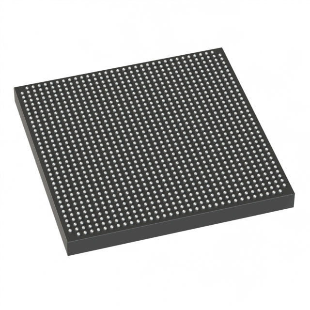
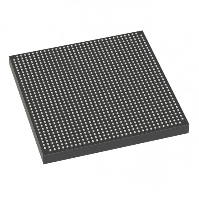
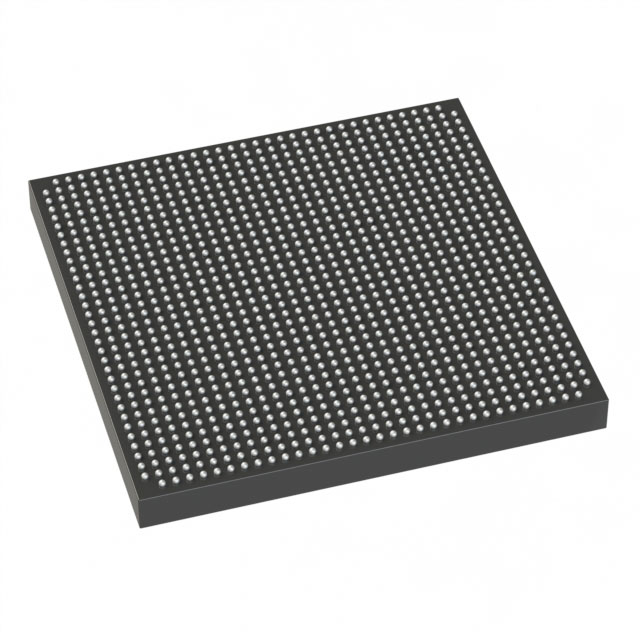
The 5SGSMD3H1F35I2G is a Stratix® V GS family FPGA in a 1152‑ball BGA (FCBGA) package, offering high logic density, substantial embedded memory, and a high I/O count for demanding digital designs. It is supplied in an industrial temperature grade and is intended for applications that require dense programmable logic, abundant on‑chip RAM, and robust I/O integration.
Key value attributes include 236,000 logic elements, approximately 13.312 Mbits of embedded memory, and 432 user I/Os, combined with a compact 1152‑FBGA (35×35) surface‑mount package and an industrial operating temperature range.
Key Features
- High Logic Density 236,000 logic elements to implement complex digital functions and large FPGA designs.
- Embedded Memory Approximately 13.312 Mbits of on‑chip RAM to support buffering, FIFOs, and data‑intensive processing.
- Abundant I/O 432 user I/Os for extensive external device interfacing and high‑pin‑count system integration.
- Package and Mounting 1152‑BBGA FCBGA package (supplier device package: 1152‑FBGA, 35×35) optimized for surface‑mount assembly and dense PCB layouts.
- Supply Voltage Core voltage range specified at 870 mV to 930 mV for core power domains.
- Industrial Temperature Grade Rated for operation from −40 °C to 100 °C to meet industrial environment requirements.
- RoHS Compliant Meets RoHS environmental requirements for lead‑free assembly.
Typical Applications
- High‑density digital processing Use the large logic resource and embedded RAM to implement intensive signal processing, packet processing, or custom compute blocks.
- Multi‑interface bridging Leverage 432 I/Os to connect multiple external peripherals, memory devices, or transceiver front ends in a single FPGA fabric.
- Industrial control and automation Industrial temperature rating and robust I/O count make this device suitable for control systems, PLCs, and factory automation logic.
- System integration and prototyping Large on‑chip resources and a compact FCBGA package enable integration of complex subsystems for evaluation and development.
Unique Advantages
- Large programmable fabric: 236,000 logic elements provide headroom for complex state machines, custom accelerators, and glue logic.
- Significant on‑chip memory: Approximately 13.312 Mbits of embedded RAM reduces reliance on external memory for many buffering and scratchpad needs.
- High I/O capacity: 432 I/Os allow broad peripheral connectivity and flexible interface routing without additional I/O expanders.
- Industrial robustness: −40 °C to 100 °C operating range supports deployment in a wide range of industrial environments.
- Compact, manufacturable package: 1152‑FBGA (35×35) surface‑mount package balances pin count and PCB real estate for production designs.
- Environmentally compliant: RoHS compliance simplifies regulatory considerations for modern electronic products.
Why Choose 5SGSMD3H1F35I2G?
The 5SGSMD3H1F35I2G is positioned for designers who require a combination of high logic density, significant embedded memory, and a large number of I/Os within a compact, industrial‑rated package. Its specifications make it suitable for complex digital systems where on‑chip resources and robust connectivity reduce board-level complexity and BOM count.
As a Stratix V GS device, it aligns with the Stratix V family documentation and electrical characterization, offering a clear set of operating parameters for system design and integration. The device’s voltage range, temperature rating, and package details provide engineering teams with verifiable constraints to plan power delivery, thermal management, and PCB layout.
Request a quote or submit an inquiry for pricing and availability to evaluate the 5SGSMD3H1F35I2G for your next FPGA‑based design.





















Date Founded: 1968
Headquarters: Santa Clara, California, USA
Employees: 130,000+
Revenue: $54.23 Billion
Certifications and Memberships: ISO9001:2015, ISO14001:2015, ISO17025:2017, ISO27001:2022, ISO45001:2018, ISO50001:2018


